Chip arrangement determining apparatus and method
- Summary
- Abstract
- Description
- Claims
- Application Information
AI Technical Summary
Benefits of technology
Problems solved by technology
Method used
Image

Examples
first embodiment
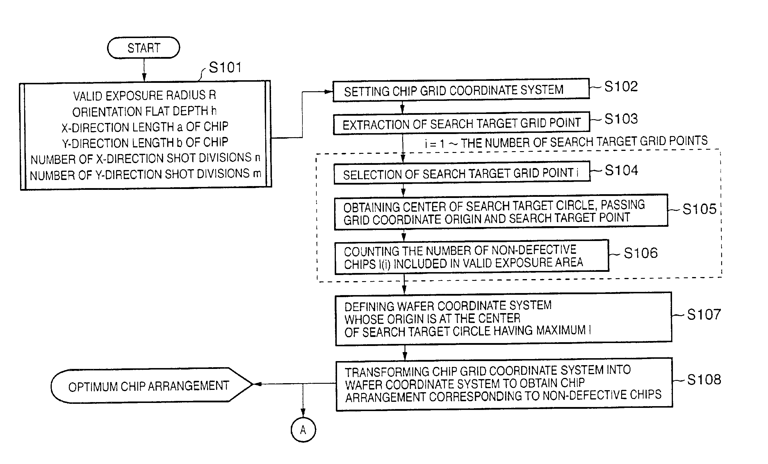
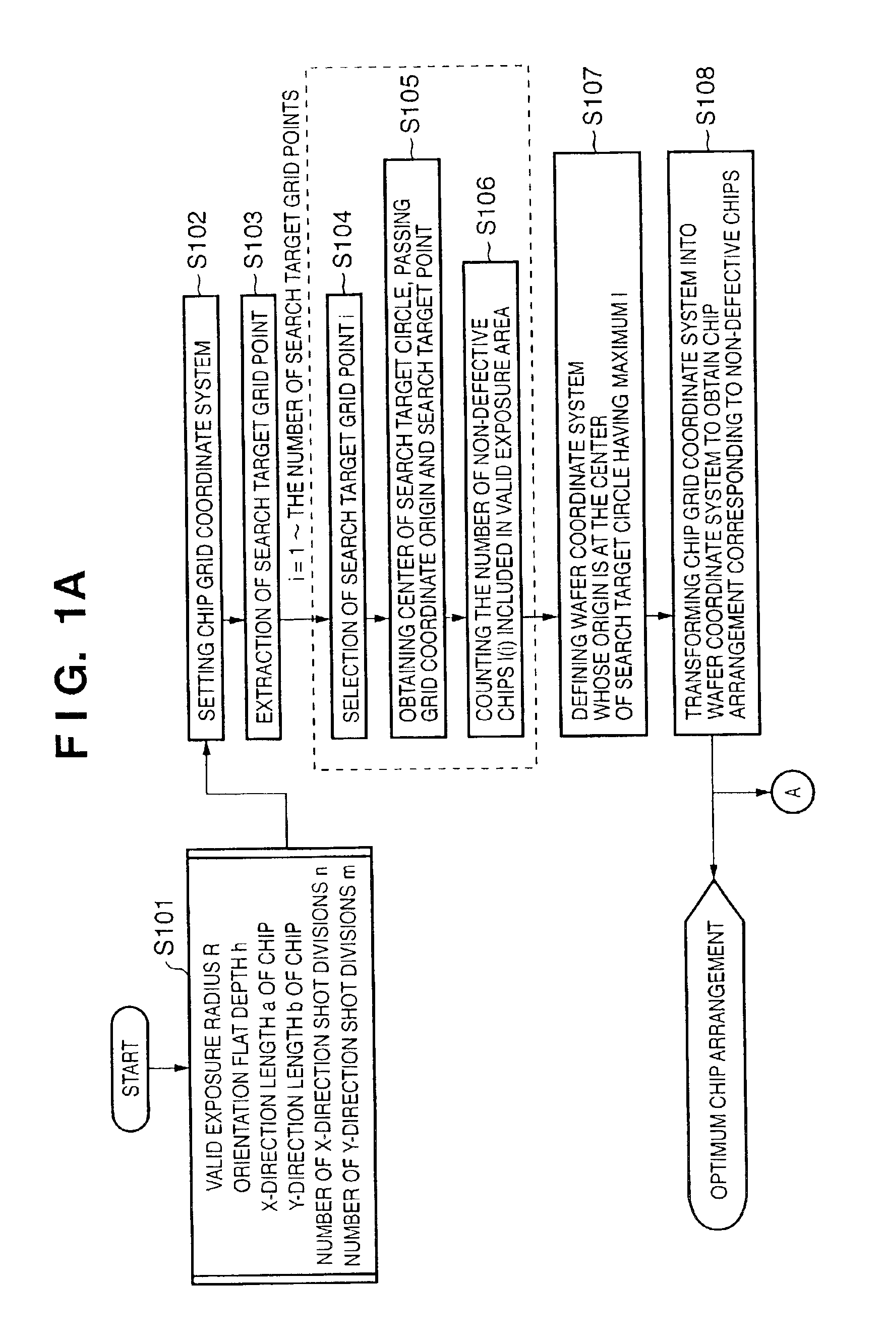
[0057]The first embodiment describes a simple example in which there is only one chip in one shot. A condition provided is as follows: a wafer diameter is 200 mm; an invalid width from an outer edge is 3 mm (i.e., diameter 2R of the valid area=194 mm); a depth of an orientation flat is 5 mm; and each of the vertical and horizontal lengths of a chip is 22 mm. Under this condition, an arrangement that maximizes the number of acquirable chips is obtained by the method according to the above-described embodiment. The result is shown in FIG. 8. According to this shot arrangement, coordinates of the center position of the top right shot are (14.65 mm, 77.20 mm) in the wafer coordinate system having its origin at the center of the wafer. The number of acquirable chips is forty-eight.
[0058]On the contrary, FIG. 9 shows an arrangement obtained by the conventional method. According to this shot arrangement, coordinates of the center position of the top right shot are (44.00 mm, 66.00 mm) in t...
second embodiment
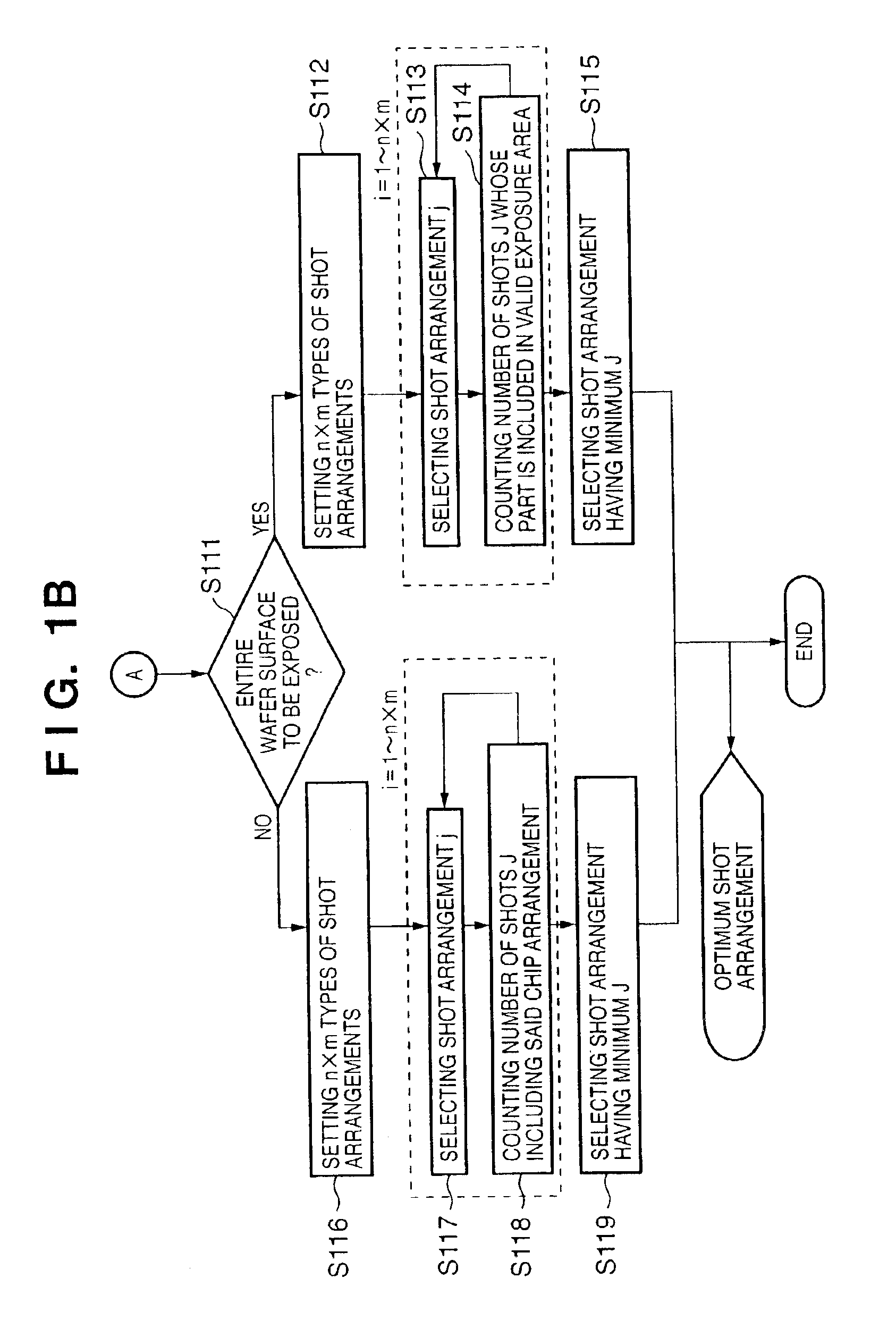
[0059]The second embodiment describes an example in which four chips (each of the vertical and horizontal lengths of each chip is 11 mm) are exposed in one shot. A condition provided is as follows: a wafer diameter is 200 mm; an invalid width from an outer edge is 3 mm; a depth or orientation flat is 5 mm; and each of the vertical and horizontal lengths of a shot is 22 mm. Under this condition, an arrangement that maximizes the number of acquirable chips and that requires the minimum number of exposure shots is obtained by the method according to the above-described embodiment. The result is shown in FIG. 10. According to this shot arrangement, coordinates of the center position of the top right shot are (43.31 mm, 77.29 mm) in the wafer coordinate system having its origin at the center of the wafer. The number of acquirable chips is 213, and the number of exposure shots is 60.
[0060]On the contrary, FIG. 11 shows an arrangement obtained by the conventional method under the above-des...
third embodiment
[0061]The third embodiment describes an example wherein six chips (each of the vertical and horizontal lengths of each chip is 11 mm) are exposed in one shot. A condition provided is as follows: a wafer diameter is 300 mm; an invalid width from an outer edge is 3 mm; no orientation flat; the vertical length of a shot is 33 mm; and the horizontal length of a shot is 22 mm. Under this condition, an arrangement that maximizes the number of acquirable chips and that requires the minimum number of exposure shots is obtained by the method according to the above-described embodiment. The result is shown in FIG. 12. According to this shot arrangement, coordinates of the center position of the top right shot are (12.00 mm, 163.00 mm) in the wafer coordinate system having its origin at the center of the wafer. The number of acquirable chips is five hundred fifteen, and the number of exposure shots is one hundred fifteen.
[0062]On the contrary, FIG. 13 shows a chip arrangement and a shot arrang...
PUM
| Property | Measurement | Unit |
|---|---|---|
| Diameter | aaaaa | aaaaa |
| Area | aaaaa | aaaaa |
Abstract
Description
Claims
Application Information
 - Generate Ideas
- Intellectual Property
- Life Sciences
- Materials
- Tech Scout
- Unparalleled Data Quality
- Higher Quality Content
- 60% Fewer Hallucinations
Browse by: Latest US Patents, China's latest patents, Technical Efficacy Thesaurus, Application Domain, Technology Topic, Popular Technical Reports.
© 2025 PatSnap. All rights reserved.Legal|Privacy policy|Modern Slavery Act Transparency Statement|Sitemap|About US| Contact US: help@patsnap.com