Structure and method for lead free solder electronic package interconnections

a technology of electronic package and structure, which is applied in the direction of soldering apparatus, semiconductor/solid-state device details, manufacturing tools, etc., can solve the problems of encapsulant walls being large, chip blm becoming molten, and subsequent reflow

Inactive Publication Date: 2005-02-15
INVENSAS CORP
View PDF46 Cites 21 Cited by
  • Summary
  • Abstract
  • Description
  • Claims
  • Application Information

AI Technical Summary

Benefits of technology

An additional advantage of the present invention is that for chip on board applications, a small amount of eutectic Sn / Ag, Sn / Cu or Sn / Ag / Cu could be used, so that the chip join reflow cycle can be maintained with a peak reflow temperature of 250° C. or less. This would be applicable to the high temp / low temp Pb-free C4 solution for direct chip on organic package situations.

Problems solved by technology

A current problem now facing the industry is that lead elimination is a strategic requirement for all manufacturers.
An additional problem is that in manufacturing, joining the chip to a first level package, typically a ceramic or organic chip carrier, is the first step.
Using a Pb free, Sn rich alloy for both first level chip join and second level module to board join creates the problem of the chip BLM becoming molten during the second level attach processes and subsequent reflows such as may be required for rework.
Another problem is that when the first level SnAgCu solder interconnect becomes completely molten inside the underfill encapsulant, it produces large hydrostatic stresses on the walls of the encapsulant.
These forces create strains large enough to cause delamination, cracking, rupture and finally, catastrophic fail of the encapsulant regions.
This would likely cause shorting between the C4 solder connections, and potentially cause opens where the C4 solder connections may break away from their original as-joined position.
Whereas other alloy systems such as AuSn 80 / 20 may be employed to produce a solder temperature hierarchy, such solutions may not be widely applicable because of various manufacturing problems.
Examples include the cost of the materials, brittle metallurgical properties and solder interactions which cause stress on the chip.

Method used


Image

  • Structure and method for lead free solder electronic package interconnections
  • Structure and method for lead free solder electronic package interconnections
  • Structure and method for lead free solder electronic package interconnections

Examples


first embodiment

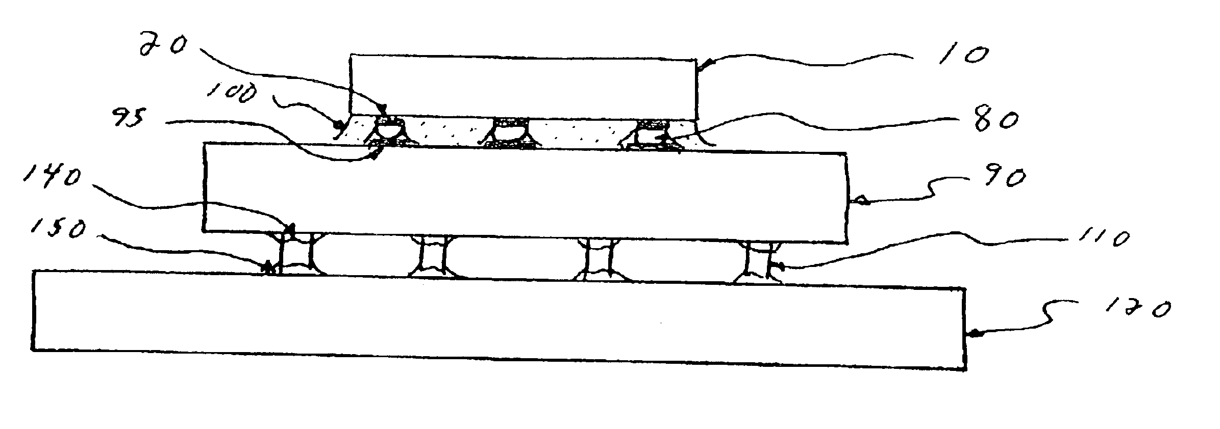
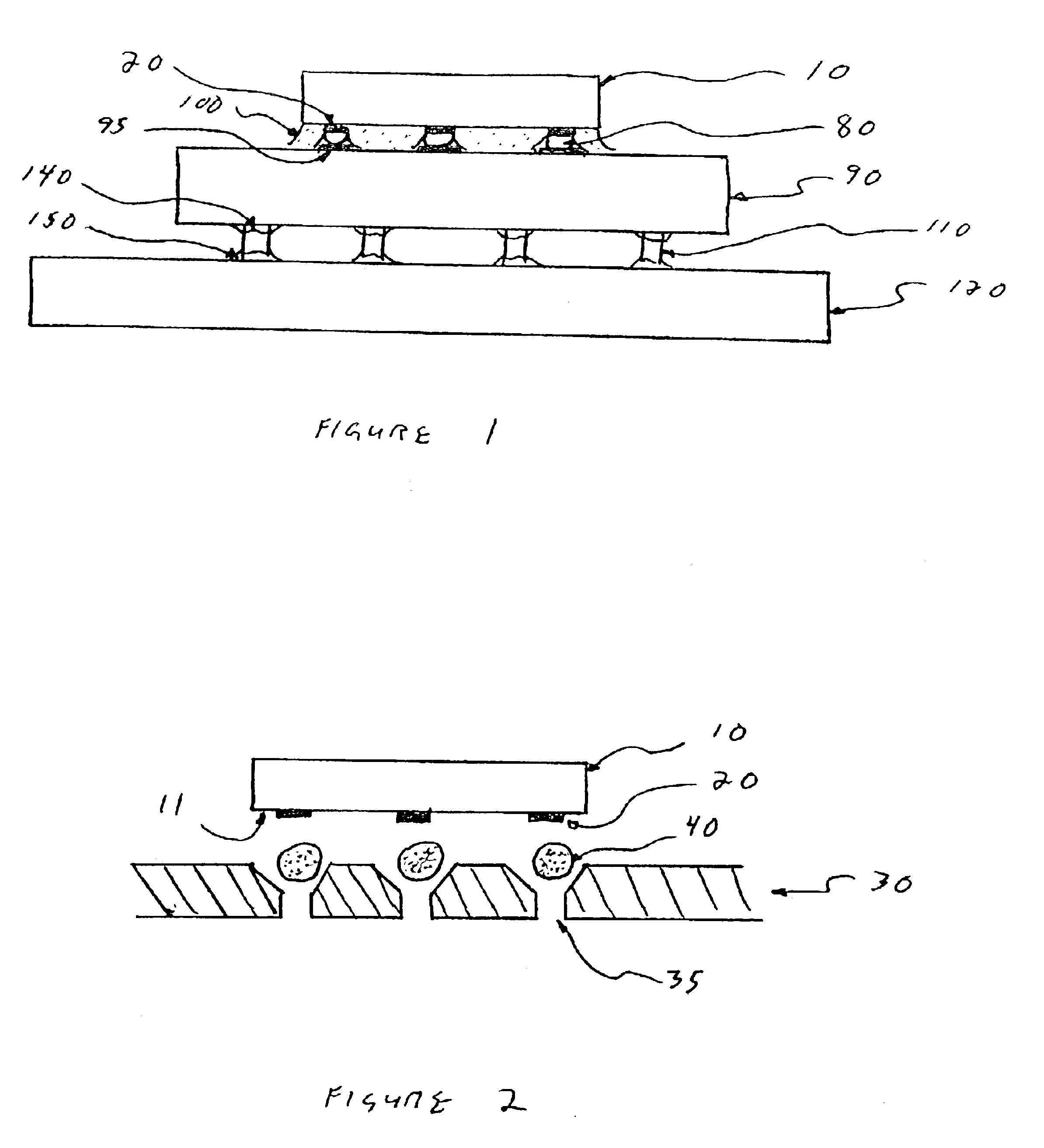
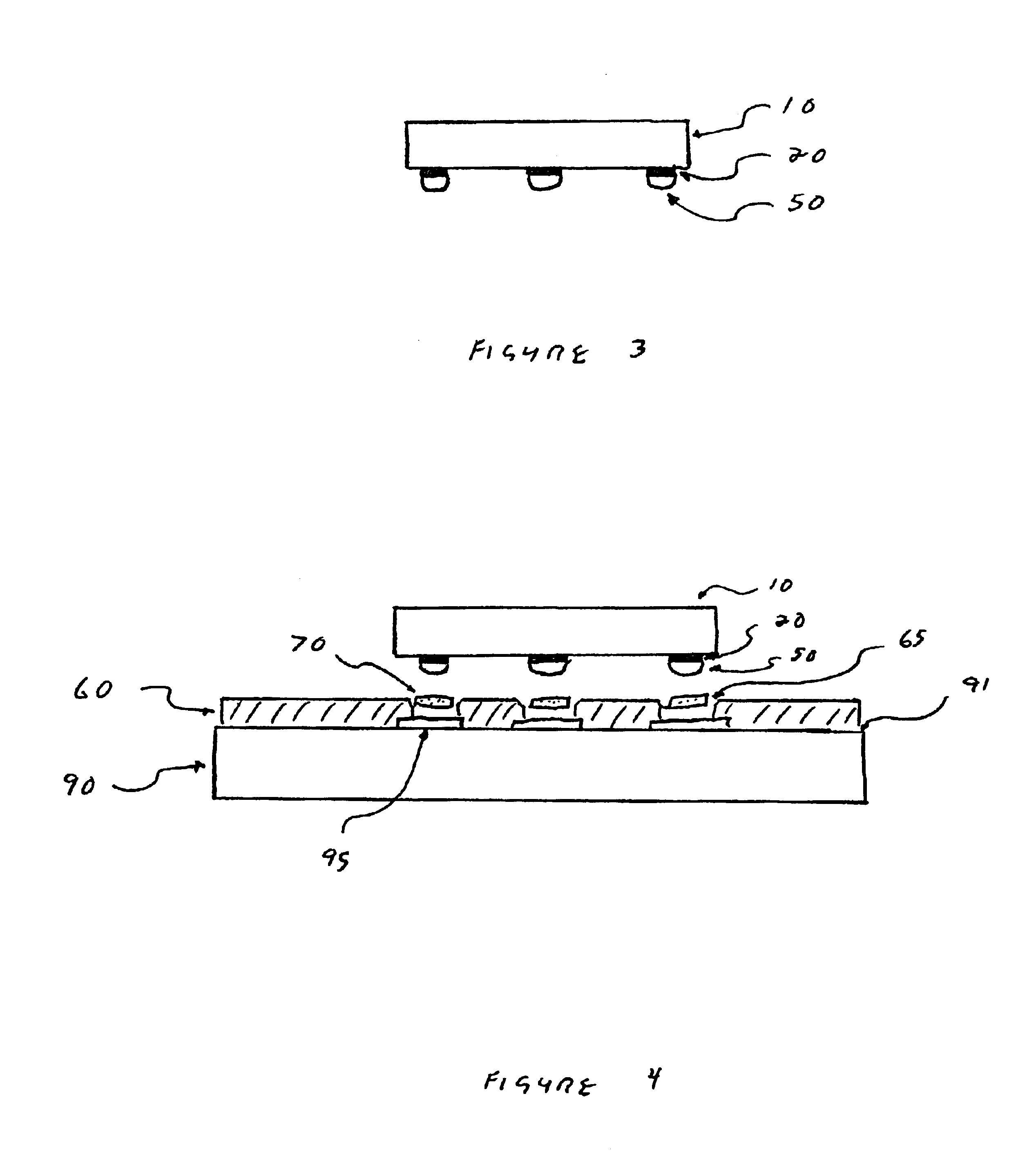
In the present invention a Sn / Ag off-eutectic lead free solder composition is provided having between about 52.0-95.0 weight % Sn and between about 48.0-5.0 weight % Ag and having inter-metallics with a melting temperature greater than 250° C. The term “inter-metallic” has its ordinary meaning of a compound with two or more metals.

In a preferred embodiment of the present invention a 72Sn / 28Ag (weight %) solder alloy is used which has a liquidus temperature of approximately 400° C. A chip join C4 reflow cycle with a peak temperature of approximately 355-375° C., with adequate dwell time typically about 1-4 minutes, will suffice to create a homogenous lead free C4 solder alloy interconnection. A homogenized solder alloy interconnection has a uniformly distributed inter-metallic phase structure.

During the subsequent second level join / assembly process, the maximum peak temperature is approximately 250° C. This temperature will create a pasty two-phase inter-metallic structure in the C4 ...

second embodiment

In the present invention a Sn / Cu off-eutectic lead free solder composition of between about 84.0-99.3 weight % Sn and between about 16.0-0.7 weight % Cu and having inter-metallics with a melting temperature greater than 250° C.

In a preferred embodiment of the present invention a 84Sn / 16Cu (in weight %) solder alloy is used which has a liquidus temperature of approximately 500° C. A chip C4 reflow cycle with a peak temperature of approximately 350-375° C., with adequate dwell time typically about 1-4 minutes, will suffice to create a homogenized C4 solder alloy interconnection. Then during the subsequent second level join / assembly process, the maximum peak temperature is approximately 250° C. This temperature will create a pasty two-phase inter-metallic structure in the C4 solder alloy interconnect, comprised of approximately 72 weight % liquid phase, and approximately 28 weight % solid phase. This alloy structure will restrict the expansion of the C4 interconnections and ensure the ...


PUM

PropertyMeasurementUnit
melting temperatureaaaaaaaaaa
temperaturesaaaaaaaaaa

Abstract

An electronic package having a solder interconnect liquidus temperature hierarchy to limit the extent of the melting of the C4 solder interconnect during subsequent second level join / assembly and rework operations. The solder hierarchy employs the use of off-eutectic solder alloys of Sn / Ag and Sn / Cu with a higher liquidus temperature for the C4 first level solder interconnections, and a lower liquidus temperature alloy for the second level interconnections. When the second level chip carrier to PCB join / assembly operations occur, the chip to chip carrier C4 interconnections do not melt completely. They continue to have a certain fraction of solids, and a lower fraction of liquids, than a fully molten alloy. This provides reduced expansion of the solder join and consequently lower stresses on the C4 interconnect.

Description

BACKGROUND OF THE INVENTIONThe present invention relates to a lead free solder structure for the assembly of electronic components, and more particularly, to a lead free solder hierarchy for use in the assembly of electronic components.Current controlled collapse chip connection (C4) or “flip chip” interconnection technology for joining chips to either ceramic or organic substrates typically employ a 97 / 3 Pb / Sn joining solder alloy as the ball-limiting metallurgy (BLM) on the chip side of the interconnect, and a suitable metallization, typically Ni / Au or Cr / Cu / Ni / Au, on the substrate side of the interconnect. This interconnect structure has to withstand temperature cycling. This temperature cycling can be a very stringent requirement, especially for chip on board interconnects where the chip is attached directly to a printed circuit board (PCB).This is because the thermal coefficient of expansion (TCE) of the chip is around 3 parts per million (ppm), and that of a typical PCB is 15-...

Claims


Application Information

Patent Timeline
Patent Type & Authority Patents(United States)
IPC IPC(8): B23K35/26H05K3/34C22C13/00H01L21/56H01L21/60H01L21/68H01L23/31H01L23/485H01L23/498H05K3/28
CPCB23K35/262H01L21/563H01L21/6835H01L23/3128H01L24/11H01L24/16H01L24/81H05K3/3463H01L2224/11334H01L23/49816H01L23/49866H01L2224/11003H01L2224/13099H01L2224/16H01L2224/73203H01L2224/73253H01L2224/8121H01L2224/81815H01L2924/01004H01L2924/01027H01L2924/01029H01L2924/0103H01L2924/01033H01L2924/01046H01L2924/01047H01L2924/01049H01L2924/01051H01L2924/01078H01L2924/01079H01L2924/01082H01L2924/01322H01L2924/01327H01L2924/15311H01L2924/01005H01L2924/01006H01L2924/01024H01L2924/0105H01L2924/01075H01L2924/014H01L2224/81024H01L2224/131H01L2224/13111B23K2201/40H01L2924/00014H01L2924/15787H01L2924/181H01L2224/05573H01L2224/05568H01L2224/056B23K2101/40H01L24/05H01L2924/00B23K35/26
Inventor FAROOQ, MUKTA G.INTERRANTE, MARIOSABLINSKI, WILLIAM
Owner INVENSAS CORP
Why Eureka
Try Eureka