This helps you quickly interpret patents by identifying the three key elements:
Problems solved by technology
Method used
Benefits of technology
Benefits of technology
Accordingly, an object of the present invention is to provide a photodetection sensor which allows electrical connection between the conductive resin and the grounding terminal to be reliably fulfilled, and which is capable of obtaining a larger electromagnetic shield effect so that the photodetection sensor can be used even under electromagnetic noise-prone environments.
Further, since this photodetection sensor does not use any separate component parts like a metal mesh, there is no need for the assembly step for separate component parts. Moreover, since the meshed conductive resin can be integrally molded by injection molding, the photodetection sensor can be manufactured with simplicity and low price and at high productivity.
Problems solved by technology
This causes a problem that the conductive resin is liable to peel off from the grounding terminal because of thermal stress due to abrupt temperature changes or the like.
This peeling, once occurred, would cause the electrical connection between the conductive resin and the grounding terminal to be insufficient, resulting in a decreased electromagnetic shield effect.
Thus, the conventional photodetection sensor has an issue that it cannot be used under environments involving much electromagnetic noise.
Therefore, there arises a need for a metal mesh, which is a separate component, involving a cost increase as well as time and labor for setting the metal mesh to the lens portion, with the result of a further issue of worse productivity.
Method used
Image
Click on the blue label to locate the original text in one second.
Reading with bidirectional positioning of images and text.
Examples
first embodiment
The First Embodiment
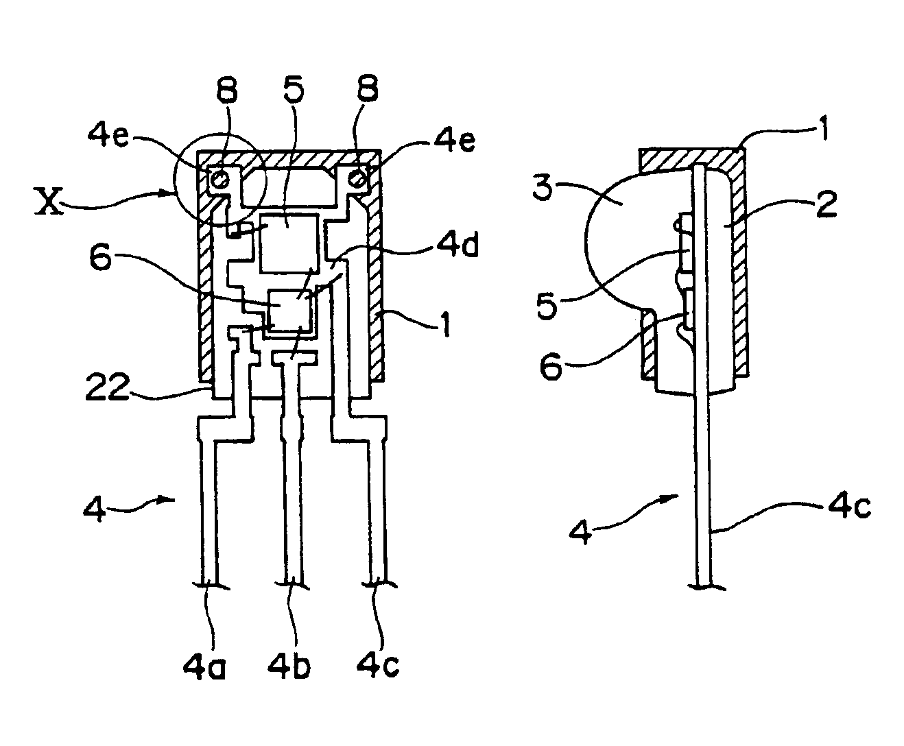
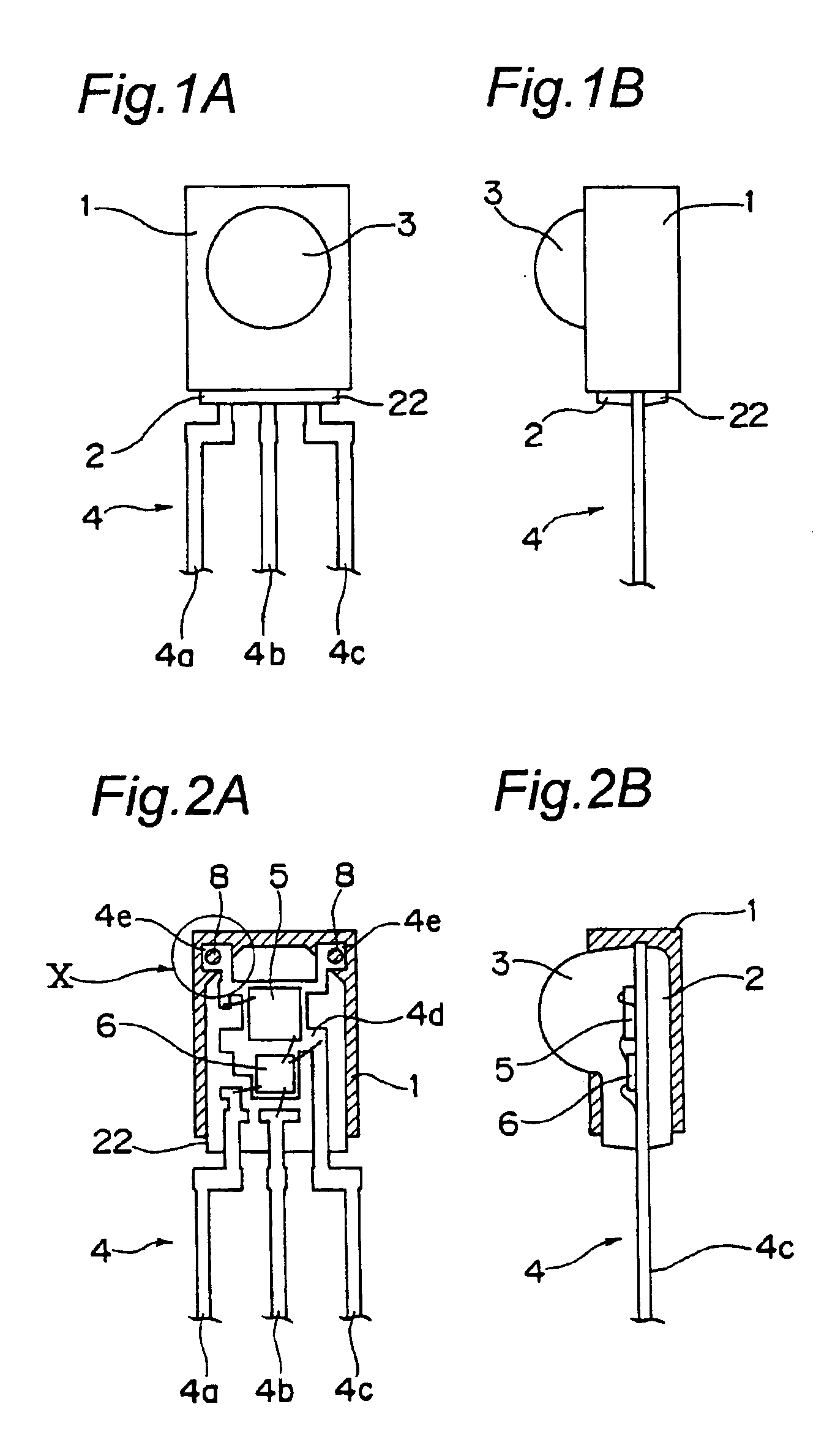
FIG. 1A is a plan view of a photodetection sensor according to a first embodiment of the present invention, and FIG. 1B is a side view of the photodetection sensor. FIG. 2A is a horizontal sectional view of the photodetection sensor, and FIG. 2B is a vertical sectional view of the photodetection sensor.
As shown in FIGS. 1A and 1B, this photodetection sensor is so constructed that part of a lead frame 4 is encapsulated in an insulative light-pervious resin 2 having a lens portion 3, and further part of this light-pervious resin 2 is encapsulated in an electrically conductive resin 1.
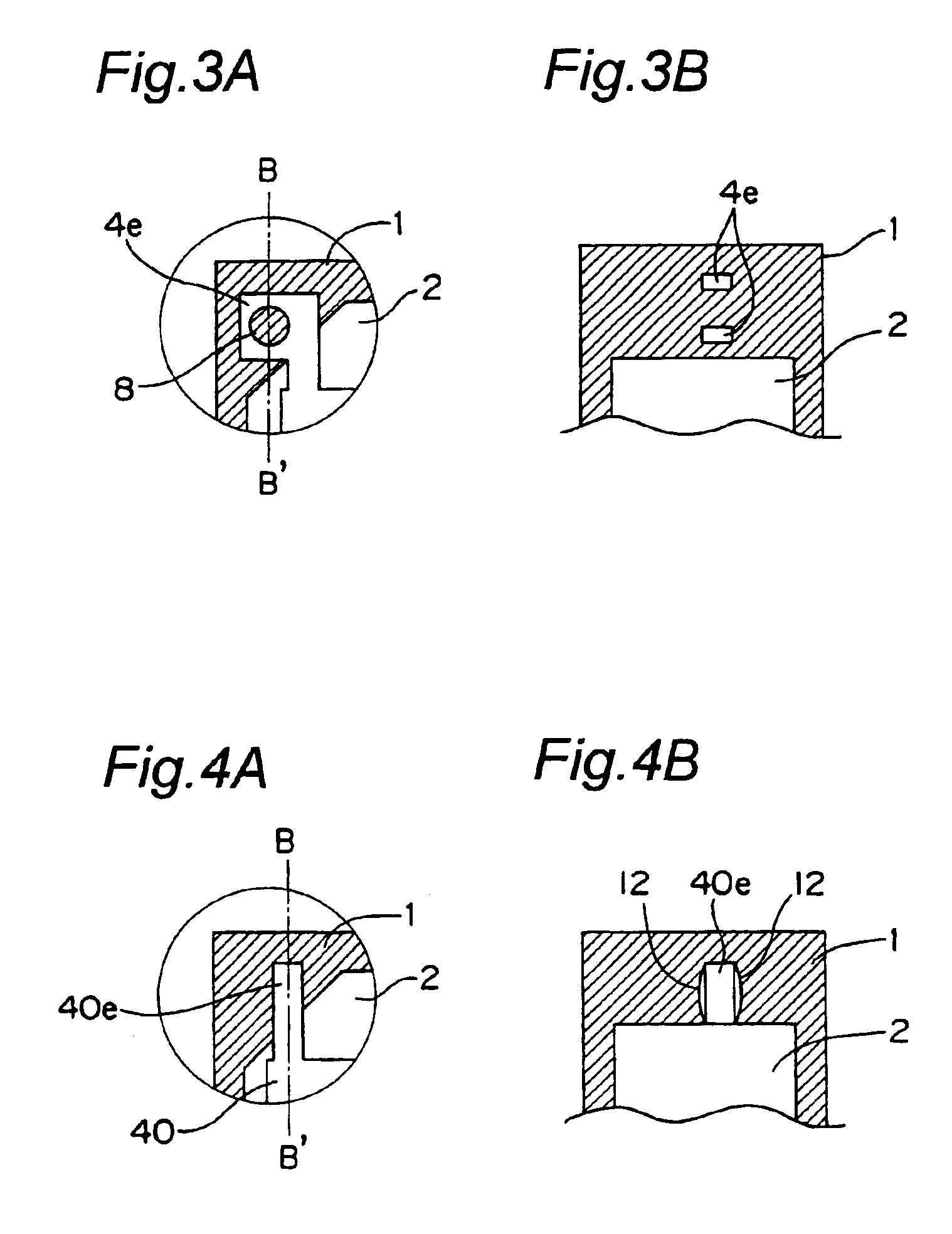
As shown in FIGS. 2A and 2B, the lead frame 4 is composed of signal input / output terminals 4a, 4b, a grounding terminal 4c, a header 4d connected to this grounding terminal 4c, and electrical connecting portions 4e, 4e extending from the header 4d toward one side reverse to the side toward which the grounding terminal 4c extends. On the surface of this header 4d, a photodetection chip ...
second embodiment
The Second Embodiment
FIG. 10A is a plan view of a photodetection sensor according to a second embodiment of the present invention, and FIG. 10B is a side view of the photodetection sensor.
In FIGS. 10A and 10B, the same constituent parts as in the photodetection sensor of the first embodiment shown in FIGS. 1 and 2 are designated by like reference numerals, and their description is omitted.
As shown in FIGS. 10A and 10B, part of the surface of the lens portion 3 is covered with a meshed electrically conductive resin 11. This conductive resin 11 is coupled to the foregoing conductive resin 1, and these conductive resins 1, 11 can be integrally molded by injection molding.
It is noted that the mesh configuration of the conductive resin 11 is not limited to the one shown in FIGS. 10A and 10B, and may be a mesh configuration given by, for example, a combination of a plurality of concentric circles and a plurality of radial lines.
In this constitution, since part of the surface of the lens p...
PUM
Abstract
A photodetection sensor allows electrical connection between conductive resin and grounding terminal to be reliably fulfilled, and is capable of obtaining a larger electromagnetic shield effect so that the photodetection sensor can be used even under electromagnetic noise-prone environments. Also, a photodetection sensor no longer necessitates a separate component metal mesh so that the photodetection sensor is low in price, simple to manufacture and high in productivity. Through holes are formed in electrical connecting portions connected to a grounding terminal via a header. The electrical connecting portions are protruded from a surface of a light-pervious resin and encapsulated in an electrically conductive resin. This conductive resin is filled into the through holes and engaged with inner surfaces of the through holes like an anchor, thus unlikely to peel off. Therefore, the grounding of the electrically conductive resin is ensured, allowing a stable electromagnetic shield effect to be obtained.
Description
This nonprovisional application claims priority under 35 U.S.C. §119(a) on Patent Application Ser. No. 2003-027968 filed in Japan on Feb. 5, 2003, the entire contents of which are hereby incorporated by reference.BACKGROUND OF THE INVENTIONThe present invention relates to a photodetection sensor to be used in various types of electronic equipment, such as TVs (Television Receivers) or VTRs (Video Tape Recorders), for use of reception of remote-control signal light.Conventionally, there has been available a photodetection sensor for remote control use, for example, as described in Japanese Unexamined Patent Application No. H09-84162. This photodetection sensor has a photodetection chip, a control-use IC chip, a chipresistor and a chip capacitor, all of which are mounted on a lead frame and encapsulated in an insulative light-pervious resin having a lens portion. Further, for shielding from electromagnetic noise, the top surface of the light-pervious resin is covered with an electric...
Claims
Application Information
Patent Timeline
Application Date:The date an application was filed.
Publication Date:The date a patent or application was officially published.
First Publication Date:The earliest publication date of a patent with the same application number.
Issue Date:Publication date of the patent grant document.
PCT Entry Date:The Entry date of PCT National Phase.
Estimated Expiry Date:The statutory expiry date of a patent right according to the Patent Law, and it is the longest term of protection that the patent right can achieve without the termination of the patent right due to other reasons(Term extension factor has been taken into account ).
Invalid Date:Actual expiry date is based on effective date or publication date of legal transaction data of invalid patent.

