Semiconductor devices and methods for fabricating the same

a technology of semiconductor devices and semiconductors, applied in the direction of semiconductor devices, basic electric elements, electrical equipment, etc., can solve the problems of high operating speed of non-type roms, high integration difficulty, and degradation of physical/electrical (device) characteristics, so as to reduce impurity diffusion

Inactive Publication Date: 2005-02-15
SAMSUNG ELECTRONICS CO LTD
View PDF8 Cites 2 Cited by
  • Summary
  • Abstract
  • Description
  • Claims
  • Application Information

AI Technical Summary

Benefits of technology

It is, therefore, a feature of the present invention to provide semiconductor devices, e.g., mask ROM devices adequate for high integration.
It is another feature, among others, of the present invention to provide methods for fabricating semiconductor devices such as mask ROM devices capable of preventing a short channel effect to be adequate for high integration.
In accordance with another embodiment of the present invention, there is provided a mask ROM device that substantially reduces diffusion of a buried impurity region. The mask ROM device comprises a buried impurity region disposed in a semiconductor substrate, a gate electrode extending across the buried impurity region, and a gate insulation layer disposed between the gate electrode and the semiconductor substrate. The gate insulation layer has a substantially uniform thickness.
Consequently, as described above, the gate insulation layer is formed before forming the buried impurity region, thereby substantially reducing impurity diffusion that can be caused by a thermal process for forming the gate insulation layer. In addition, because the gate insulation layer is covered with a conductive layer, the gate insulation layer can be prevented from being recessed during processing steps such as ion implantation or cleaning.

Problems solved by technology

On the other hand, the NOR-type ROM has a high operating speed, but is not suitable for high integration due to its great unit cell area.
That is, the buffer oxide layer 20 may suffer from an increase in thickness deviation as well as degradation of physical / electrical (device) characteristics.
The thermal oxidization process is typically conducted at approximately 850° C. Such a high-temperature thermal oxidization may, however, cause diffusion of impurities in the impurity region 50.
As a result, the distance 11 between the adjacent buried impurity regions 55 is reduced, causing a short channel effect, impeding high integration of semiconductor devices.

Method used


Image

  • Semiconductor devices and methods for fabricating the same
  • Semiconductor devices and methods for fabricating the same
  • Semiconductor devices and methods for fabricating the same

Examples


Embodiment Construction

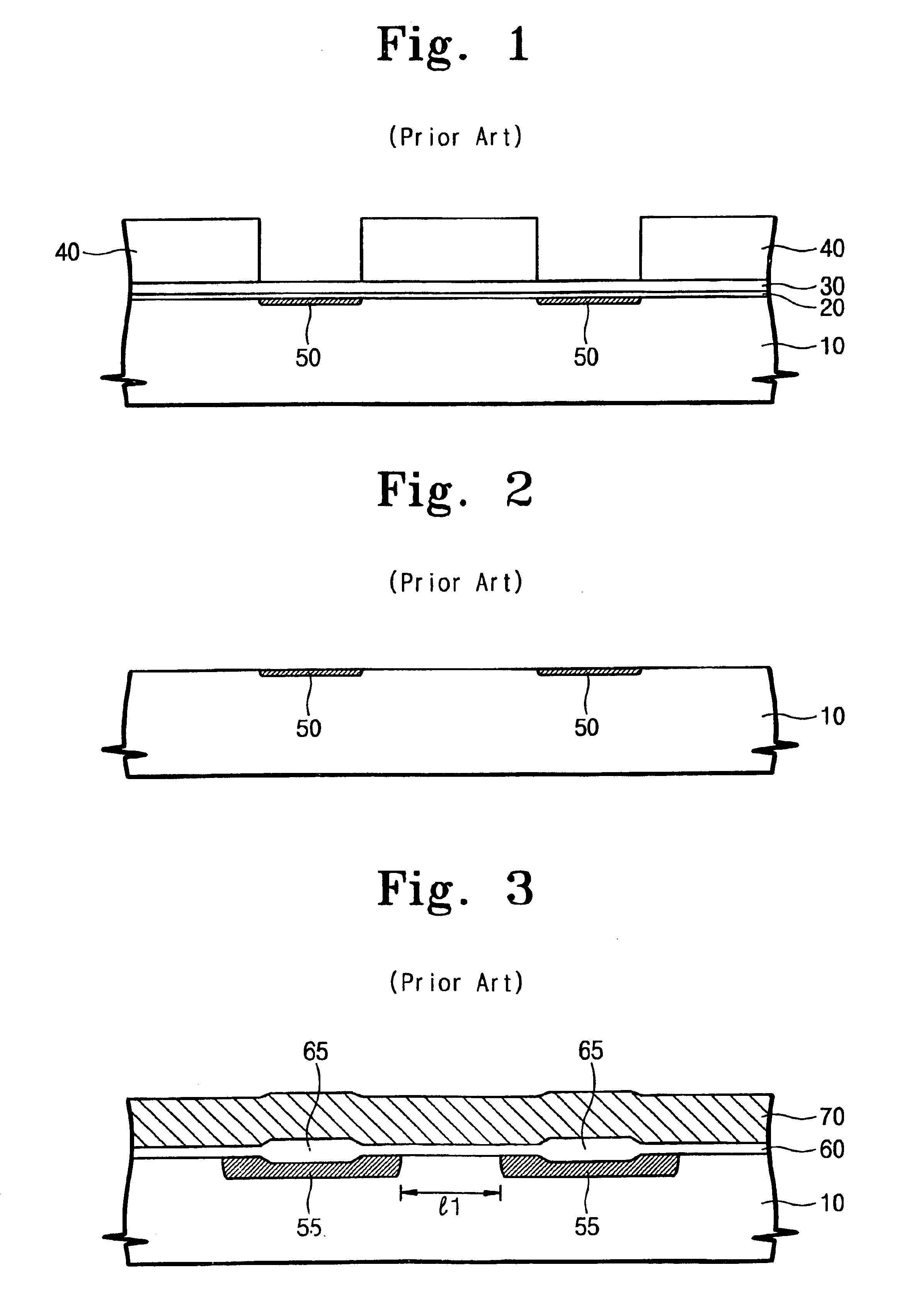
The present invention will now be described more fully hereinafter with reference to the accompanying drawings, in which preferred embodiments of the invention are shown. The invention may, however, be embodied in different forms and should not be construed as limited to the embodiments set forth herein. Rather, these embodiments are provided so that this disclosure will be thorough and complete, and will fully convey the scope of the invention to those skilled in the art. In the drawings, the thickness of layers and regions are exaggerated for clarity. It will also be understood that when a layer is referred to as being “on” another layer or substrate, it can be directly on the other layer or substrate, or intervening layers may also be present. Like numbers refer to like elements throughout.

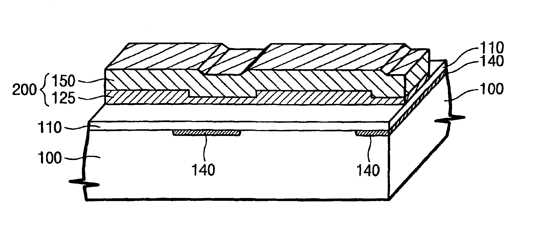
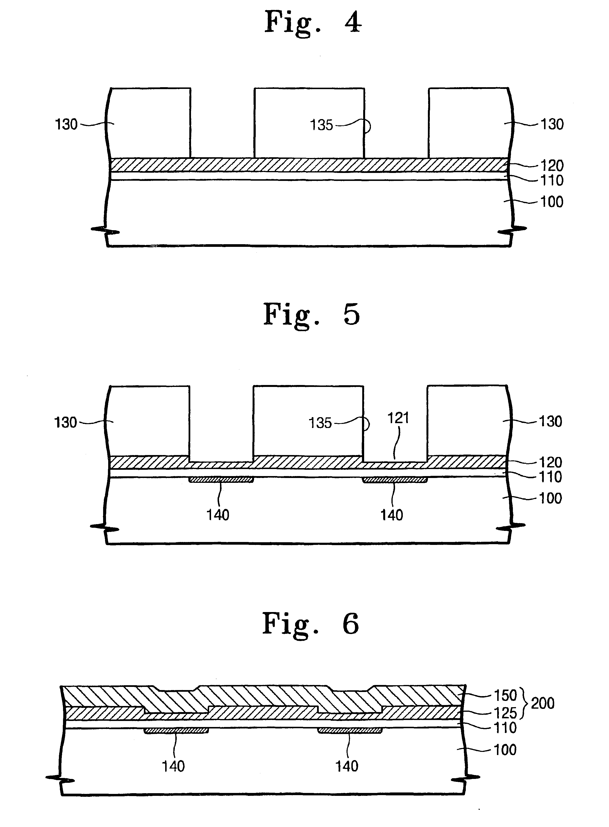
FIGS. 4 to 6 are cross-sectional views illustrating a method for fabricating a mask ROM semiconductor device according to an embodiment of the present invention.

Referring to FIG. 4, a device is...


PUM

PropertyMeasurementUnit
temperatureaaaaaaaaaa
thicknessaaaaaaaaaa
concentrationaaaaaaaaaa

Abstract

Disclosed are semiconductor devices and methods for fabricating the same. According to one embodiment, the method includes sequentially forming a gate insulation layer and a conductive layer on a semiconductor substrate. A buried impurity region is then formed in the semiconductor substrate. Thus, the gate insulation layer is formed before forming the buried impurity region, thereby substantially reducing impurity diffusion that can be caused by a thermal process for forming the gate insulation layer. In addition, the gate insulation layer is not exposed, thus protecting the gate insulation layer from being recessed.

Description

RELATED APPLICATIONThis application relies for priority upon Korean Patent Application No. 2002-03871, filed on Jan. 23, 2002, the contents of which are herein incorporated by reference in their entirety.BACKGROUND OF THE INVENTION1. Field of the InventionThe present invention relates to semiconductor devices and methods of fabricating the same.2. Description of the Related ArtMask ROMs are largely divided into NAND-type ROMs and NOR-type ROMs. While the NAND-type ROM has a slow operating speed, it is adequate for high integration due to its small unit cell area. On the other hand, the NOR-type ROM has a high operating speed, but is not suitable for high integration due to its great unit cell area. Therefore, a flat NOR-type ROM structure, which enables both a high operating speed of the NOR-type ROM and a small cell area of the NAND-type ROM, has been proposed. The flat NOR-type ROM is a type of mask ROMs in which a device isolation layer and a contact plug are not included in a un...

Claims


Application Information

Patent Timeline
Patent Type & Authority Patents(United States)
IPC IPC(8): H01L21/70H01L21/265H01L21/02H01L27/112H01L21/8246H01L21/8234
CPCH01L21/2652H01L27/1126H01L27/112H01L21/823462H10B20/383H10B20/00H10B99/00
Inventor KANG, MIN-KYURYU, WON-HYUNG
Owner SAMSUNG ELECTRONICS CO LTD
Why Eureka
Try Eureka