Vertical bipolar transistor formed using CMOS processes

Inactive Publication Date: 2005-02-22
TEXAS INSTR INC
View PDF1 Cites 3 Cited by
  • Summary
  • Abstract
  • Description
  • Claims
  • Application Information

AI Technical Summary

Benefits of technology

An important technical advantage of the present invention inheres in the fact that implant processes which are used to form field effect devices on an integrated substrate can also be used to form vertical bipolar devices on the same substrate. In this manner, bipolar transistors can be used with both pMOS and nMOS field effect devices to create complex BiCMOS circuitry without incurring the complexity and costs associated with conventional techniques for forming these structures.
An important technical adv

Problems solved by technology

Unfortunately, the use of implant processes to form field effect devices and then subsequent implant processes to form bipolar devices greatly increases the cost and complexity of the formation of the device.
These techniques have been somewhat successful but they have been limited principally because bipolar devices require two junctio

Method used


Image

  • Vertical bipolar transistor formed using CMOS processes
  • Vertical bipolar transistor formed using CMOS processes
  • Vertical bipolar transistor formed using CMOS processes

Examples


Embodiment Construction

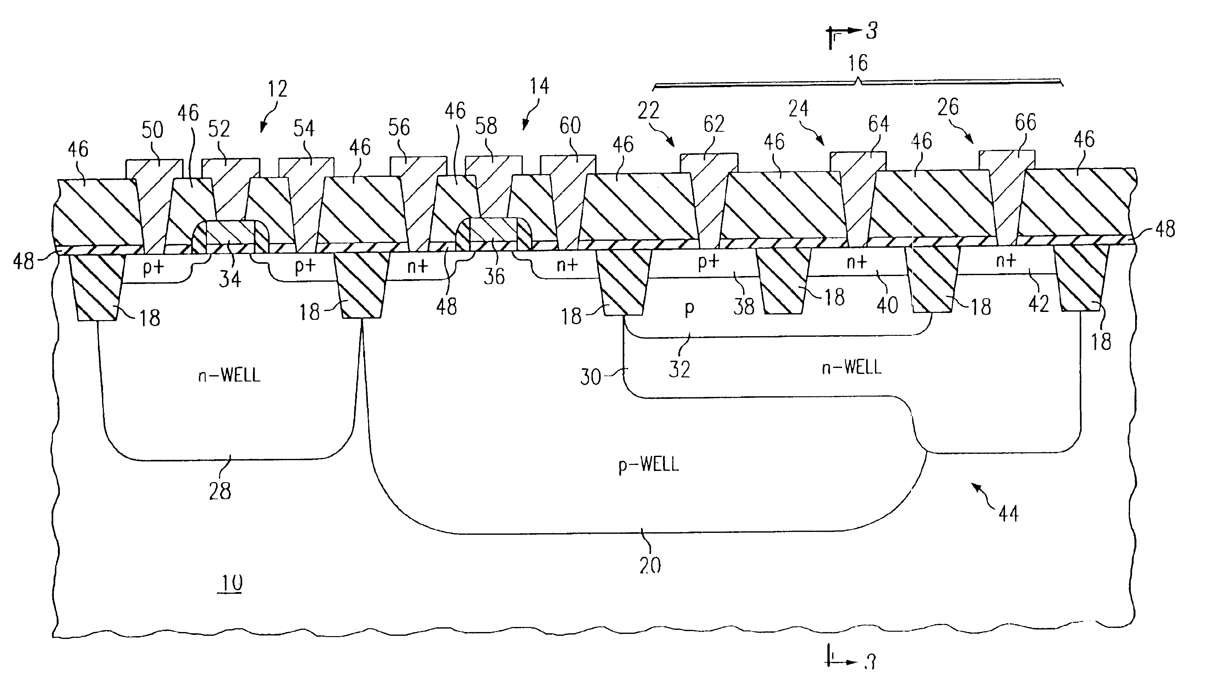
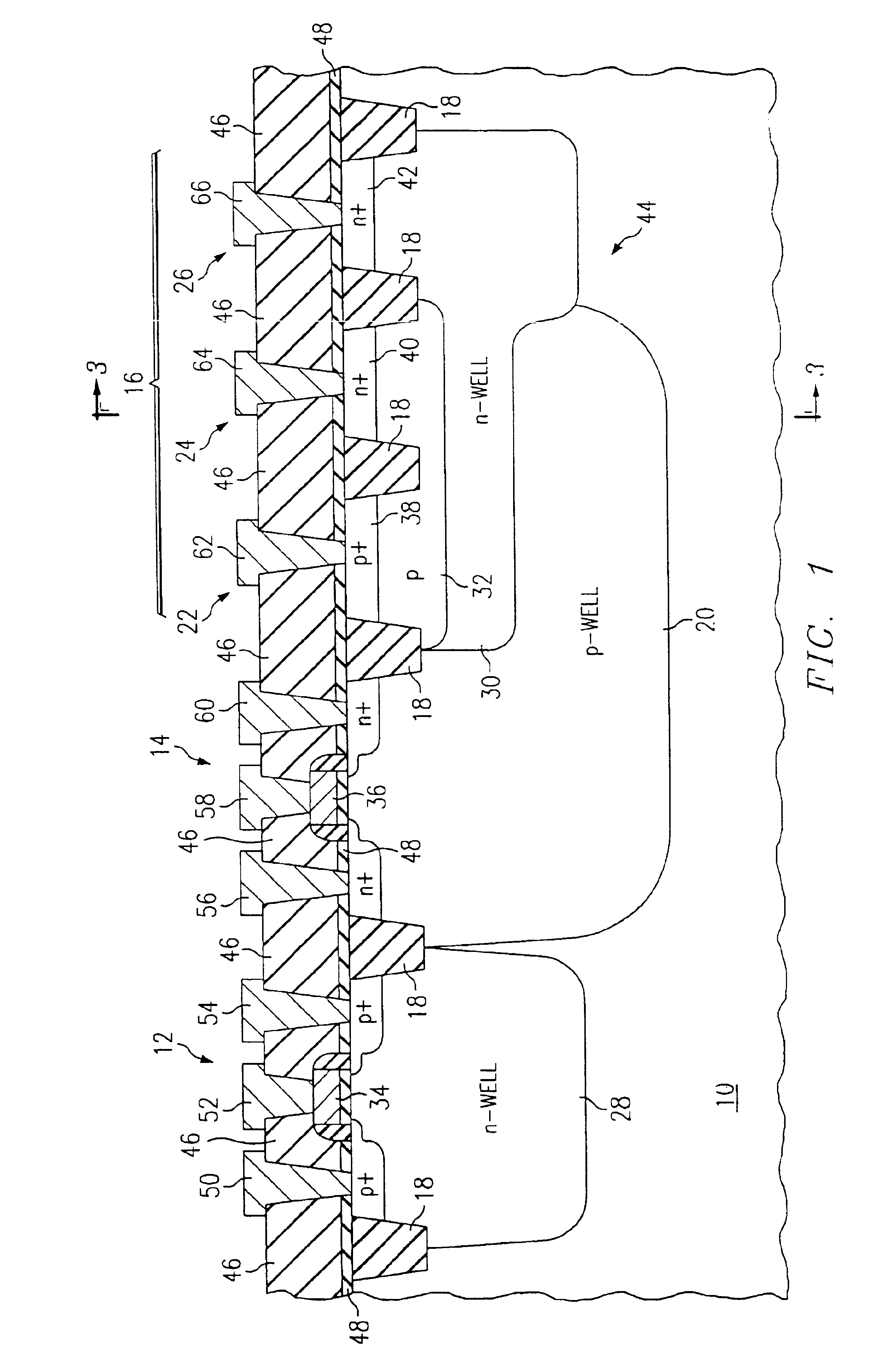
FIG. 1 is an elevational diagram illustrating the completed structure of a number of transistors constructed on a semiconductor substrate 10. According to one embodiment of the present invention, the substrate 10 may comprise a background p-type doping such that the substrate exhibits resistivity on the order of between 2 to 10 ohm-cm. FIG. 1 illustrates a completed pMOS field effect transistor indicated generally at 12, a completed nMOS field effect transistor indicated generally at 14 and a vertical bipolar transistor indicated generally at 16.

The transistors 12, 14 and 16 are formed in the outer surface of substrate 10 by first isolating active regions from each other using trench isolation structures indicated at 18 in FIG. 1. Trench isolation structures 18 are formed by photolithographically patterning the outer surface substrate 10. Trenches are then formed in the outer surface of substrate 10. These trenches are then filled with a dielectric which may comprise, for example, s...


PUM


Abstract

A vertical bipolar transistor is described which utilizes ion implantation steps which are used to form an nMOS field effect device and a pMOS field effect device. The implantation steps form an n-well, a channel stop p-well region and emitter region which are vertically oriented within a semiconductor substrate. The resulting bipolar device is junction isolated from other circuits formed on the substrate by a p-well region.

Description

TECHNICAL FIELD OF THE INVENTIONThis invention relates in general to the field of integrated electronic systems and more particularly to the architecture and formation of a vertical bipolar transistor constructed using adjunct CMOS processes.BACKGROUND OF THE INVENTIONThe construction of field effect devices in CMOS technologies involves the use of sequential implant processes to form conductive and semiconductive regions within the outer surface of a semiconductor substrate. These implant processes are optimized to enable the field effect devices to function in complimentary fashion. P-channel devices and n-channel devices are formed on the same substrate using photolithographic processes to cover certain of the devices while implant processes are performed on the remaining devices.State of the art bipolar transistors require different implant and photolithographic masking processes. Many integrated architectures require or may be optimized if the integrated system can utilize both...

Claims


Application Information

Patent Timeline
IPC IPC(8): H01L21/70H01L29/66H01L31/102H01L21/8238H01L31/072H01L31/0264H01L31/0336H01L29/76H01L31/06H01L31/0328H01L31/109H01L21/8249H01L27/06
CPCH01L27/0623H01L21/8249
Inventor CHATTERJEE, AMITAVA
Owner TEXAS INSTR INC
Why Eureka
Try Eureka