

Nitride semiconductor light-emitting device and optical device including the same
a technology of semiconductor light-emitting devices and optical devices, which is applied in the direction of semiconductor lasers, lasers, solid-state devices, etc., can solve the problems of reducing luminous efficiency, difficult to form an emission layer having excellent crystallinity, and unstable chemical thermal equilibrium state of the ingan layer
- Summary
- Abstract
- Description
- Claims
- Application Information
AI Technical Summary
Benefits of technology
Problems solved by technology
Method used
Image

Examples
embodiment 1
[0042
[0043]In a nitride semiconductor light-emitting device according to Embodiment 1 of the present invention, it is possible to reduce crystal system separation by introducing Al into a single quantum layer of GaN1-x−y−zAsxPySbz (where 01-x−y−zAsxPySbz single well layer (where 0<x+y+z≦0.3).
[0044]As to Composition Ratio of As, P or Sb in Single Well Layer
[0045]The total composition ratio x+y+z of As, P and Sb in the AlGaN1-x−y−zAsxPySbz single well layer in the nitride semiconductor light-emitting device is preferably set to at least 0.01% and not more than 30%, and more preferably at least 0.1% and not more than 10%. If the composition ratio x+y+z is smaller than 0.01%, it is difficult to attain improvement of luminous intensity by introducing As, P or Sb into the single well layer. If the composition ratio x+y+z is higher than 30%, on the other hand, it is difficult to reduce crystal system separation caused by As, P or Sb even if Al is added to the single well layer. If the comp...
embodiment 2
[0079
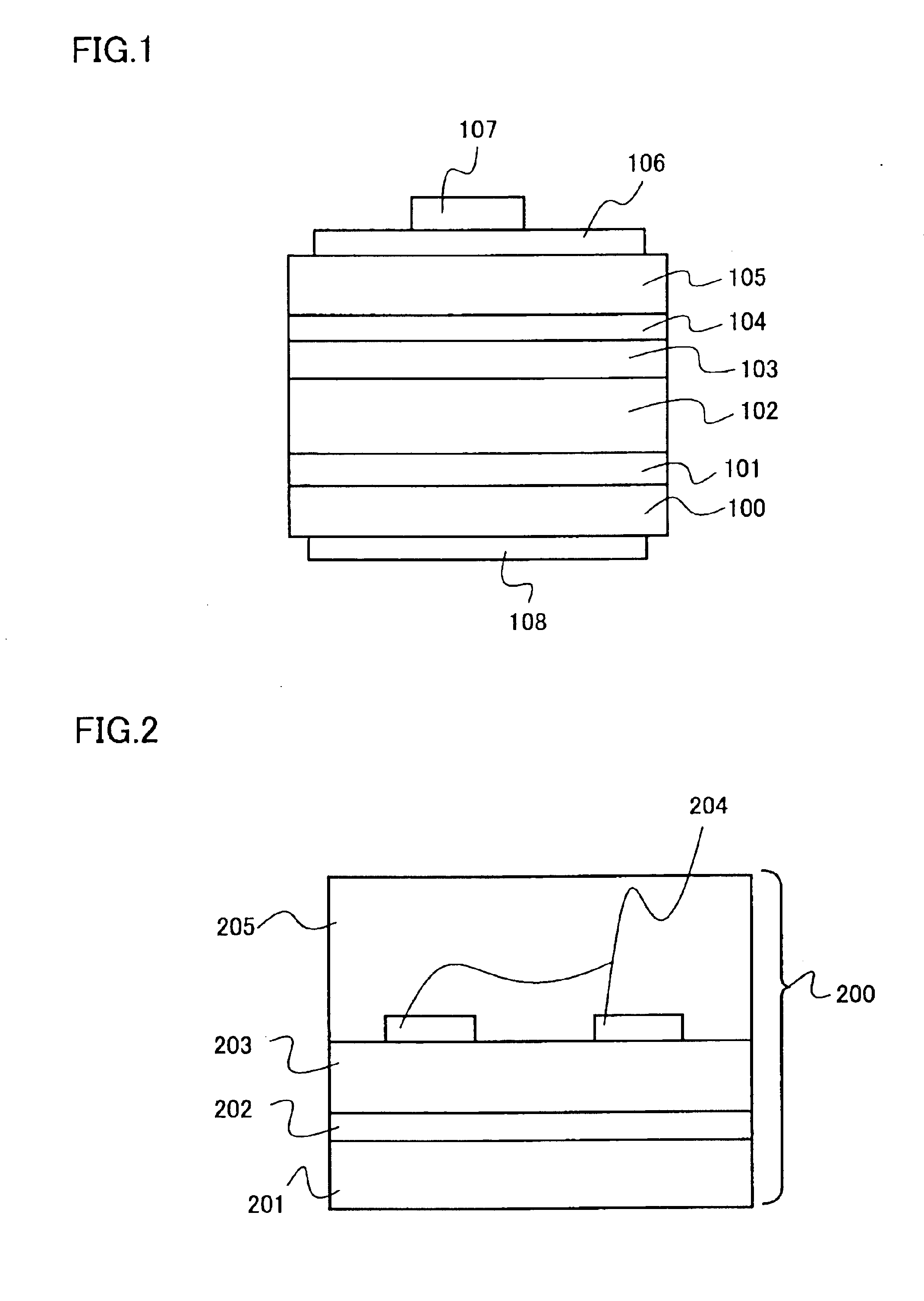
[0080]Embodiment 2 is different from Embodiment 1 only in a point that the GaN substrate 100 of FIG. 1 is replaced with a pseudo GaN substrate 200 of FIG. 2 or a pseudo GaN substrate 200a of FIG. 3B while a p electrode and an n electrode are formed on the same side of the substrate as shown in FIG. 4.
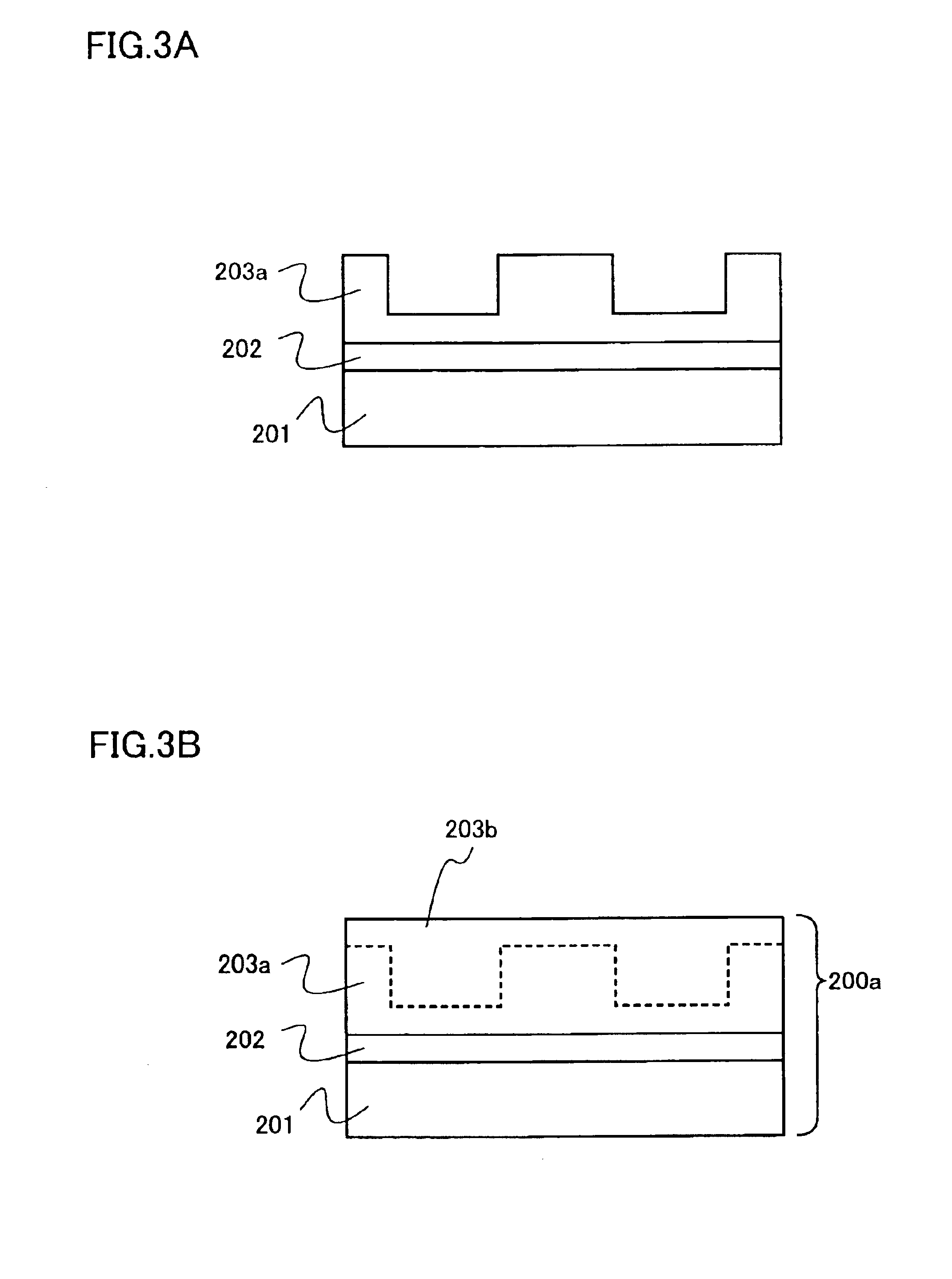
[0081]The pseudo GaN substrate 200 shown in FIG. 2 includes a seed substrate 201, a low-temperature buffer layer 202, an n-type GaN layer 203, a growth inhibitor film 204 and an n-type GaN thick film 205.
[0082]The seed substrate 201 is used as a base for growing the n-type GaN thick film 205. The term “growth inhibitor film” denotes a film on which no nitride semiconductor layer grows directly. The pseudo GaN substrate is not restricted to the structure shown in FIG. 2 but this term denotes a substrate including at least a seed substrate and a growth inhibitor film.
[0083]The pseudo GaN substrate 200a shown in FIG. 3B includes a seed substrate 201, a low-temperature buffer layer 202...
embodiment 3
[0088
[0089]Embodiment 3 is different from Embodiment 1 only in a point that a nitride semiconductor light-emitting diode is formed on a substrate other than a nitride semiconductor substrate through a nitride semiconductor buffer layer while a p electrode and an n electrode are formed on the same side of the substrate.
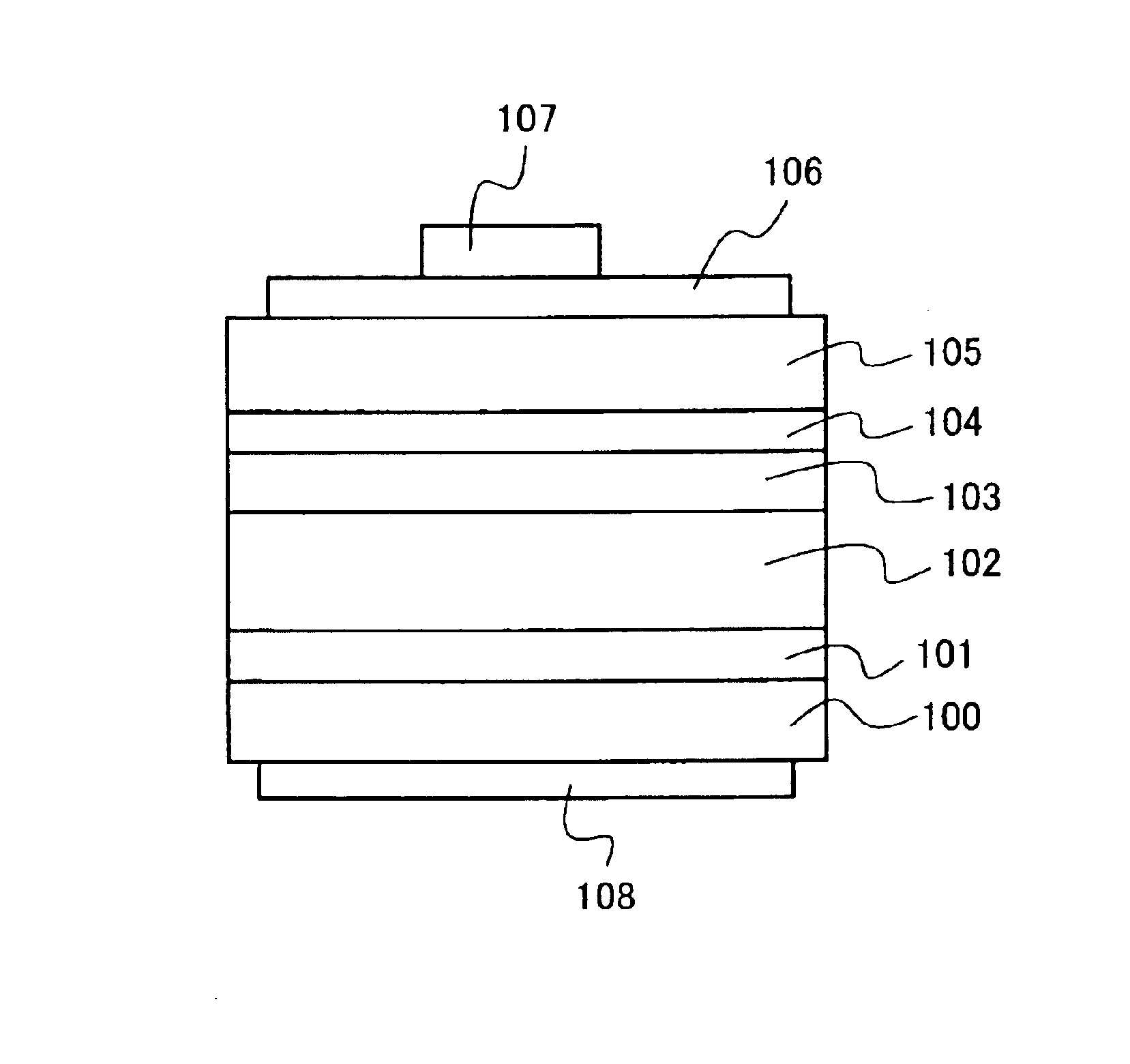
[0090]FIG. 4 shows the nitride semiconductor light-emitting diode according to Embodiment 3 as a schematic sectional view, and FIG. 5 shows a top plan view corresponding to FIG. 4. The diode device shown in FIG. 4 includes a C-plane {0001} sapphire substrate 300, a low-temperature GaN buffer layer 101 (thickness: 25 nm), an n-type GaN layer 102, a single well layer 103, a p-type Al0.1Ga0.9N carrier blocking layer 104, a p-type GaN contact layer 105, an optically transparent electrode 106, a p electrode 107, an n electrode 108 and a dielectric film 109.
[0091]The nitride semiconductor light-emitting diode grown on the substrate (sapphire substrate) other than a nitride s...
PUM
 Abstract
Description
Claims
Application Information