Post-deposition treatment to enhance properties of Si-O-C low films

a technology of low film and post-deposition treatment, which is applied in the direction of chemical vapor deposition coating, semiconductor/solid-state device details, coatings, etc., can solve the problems of degrading the properties of the film, increasing the dielectric constant of the film, and absorbing moisture, so as to improve the adhesion and reduce the shrinkage of the deposited film. , the effect of enhancing the stability of the film

Inactive Publication Date: 2005-02-22
APPLIED MATERIALS INC
View PDF20 Cites 18 Cited by
  • Summary
  • Abstract
  • Description
  • Claims
  • Application Information

AI Technical Summary

Benefits of technology

The method of the present invention provides a new and improved post-deposition treatment process. The method of the present invention deposits and densifies and cures an insulating layer. The post-deposition densification treatment further enhances adhesion by reducing shrinkage of the deposited film. The post-deposition densification takes place in a reducing environment. In one embodiment, the deposited film is treated in a reducing environment of ammonia for approximately 1 to 5 minutes at a temperature of approximately 400° C. Curing can be done in either a vacuum or conventional furnace environment. The densification is particularly useful for enhancing the stability of a film that is to be cured ex-situ, i.e. after removing the substrate from vacuum.
The method is particularly useful in the manufacture of sub-0.2 micron circuits as it can form a PMD or IMD film with a dielectric constant below 3.0. The film has good gap fill capabilities, high film stability and etches uniformly and controllably when subject to a chemical mechanical polishing (CMP) step. The method is particularly useful when, for throughput reasons, the substrate containing the deposited film is removed from vacuum for curing in a furnace.

Problems solved by technology

Consequently, the film tends to absorb moisture.
The absorbed moisture generally degrades the properties of the film.
In the case of a low-k film, moisture tends to increase the dielectric constant of the film and is detrimental to film adhesion.

Method used


Image

  • Post-deposition treatment to enhance properties of Si-O-C low films
  • Post-deposition treatment to enhance properties of Si-O-C low films
  • Post-deposition treatment to enhance properties of Si-O-C low films

Examples


Embodiment Construction

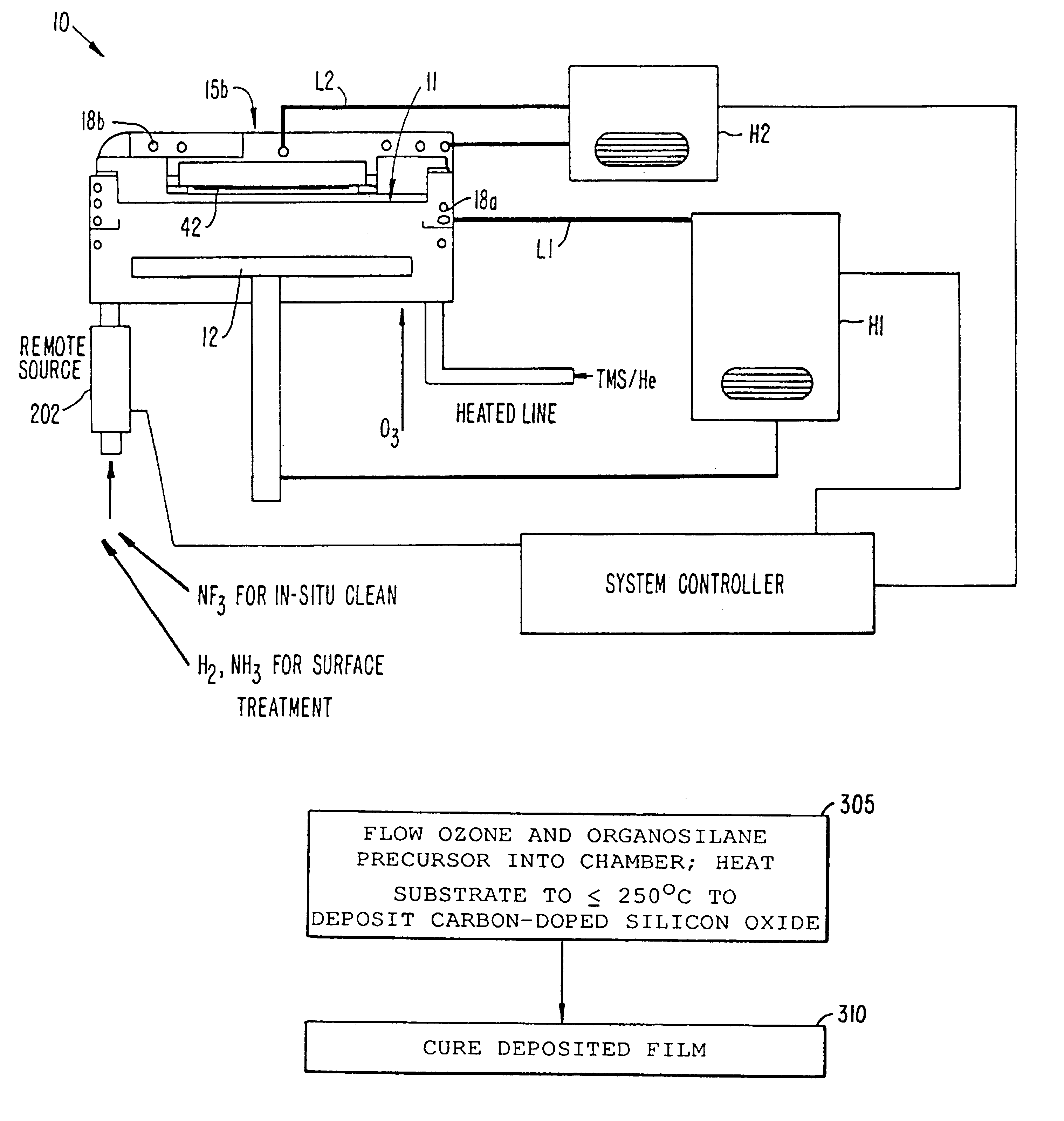
I. Exemplary CVD System

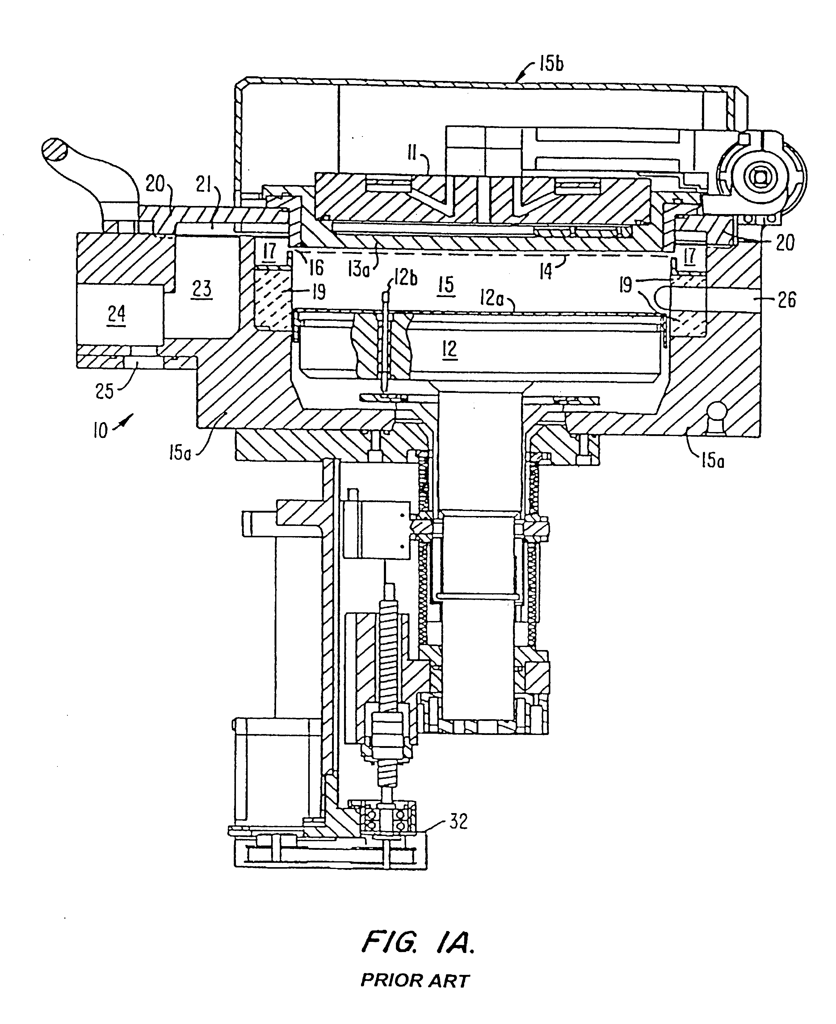
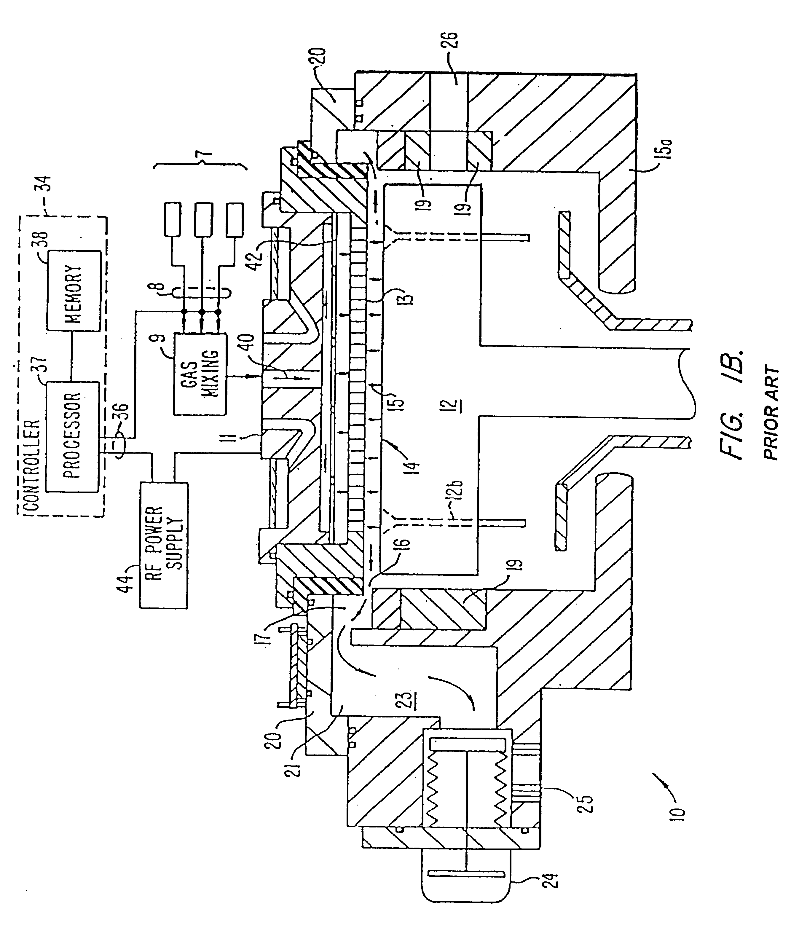
One suitable CVD apparatus in which the method of the present invention can be carried out is shown in FIGS. 1A and 1B, which are vertical, cross-sectional views of a CVD system 10, having a vacuum or processing chamber 15 that includes a chamber wall 15a and chamber lid assembly 15b. Chamber wall 15a and chamber lid assembly 15b are shown in exploded, perspective views in FIGS. 1C and 1D.

CVD system 10 contains a gas distribution manifold 11 for dispersing process gases to a substrate (not shown) that rests on a heated pedestal 12 centered within the process chamber. During processing, the substrate (e.g. a semiconductor wafer) is positioned on a flat (or slightly convex) surface 12a of pedestal 12. The pedestal can be moved controllably between a lower loading / off-loading position (depicted in FIG. 1A) and an upper processing position (indicated by dashed line 14 in FIG. 1A and shown in FIG. 1B), which is closely adjacent to manifold 11. A centerboard (not sh...


PUM

PropertyMeasurementUnit
temperatureaaaaaaaaaa

Abstract

A method for providing a dielectric film having enhanced adhesion and stability. The method includes a post deposition treatment that densifies the film in a reducing atmosphere to enhance stability if the film is to be cured ex-situ. The densification generally takes place in a reducing environment while heating the substrate. The densification treatment is particularly suitable for silicon-oxygen-carbon low dielectric constant films that have been deposited at low temperature.

Description

BACKGROUND OF THE INVENTIONThe present invention relates to the formation of dielectric layers during fabrication of integrated circuits on semiconductor wafers. More particularly, the present invention relates to a method for providing a dielectric film having a low dielectric constant that is particularly useful as a premetal or intermetal dielectric layer.One of the primary steps in the fabrication of modem semiconductor devices is the formation of a thin film on a semiconductor substrate by chemical reaction of gases. Such a deposition process is referred to as chemical vapor deposition or “CVD.” Conventional thermal CVD processes supply reactive gases to the substrate surface where heat-induced chemical reactions take place to produce a desired film. Plasma enhanced CVD techniques, on the other hand, promote excitation and / or dissociation of the reactant gases by the application of radio frequency (RF) or microwave energy. The high reactivity of the released species reduces the...

Claims


Application Information

Patent Timeline
Patent Type & Authority Patents(United States)
IPC IPC(8): C23C16/56C23C16/02C23C16/40H01L21/02H01L21/316H01L21/3105H01L21/314
CPCC23C16/0218C23C16/56H01L21/02071H01L21/02126H01L21/02203H01L21/02211H01L21/02271H01L21/02274H01L21/02312H01L21/02337H01L21/0234H01L21/02362H01L21/3105H01L21/31604H01L21/31612H01L21/31633H01L21/76826H01L21/76837C23C16/401Y10S438/931H01L21/3146H01L21/76807
Inventor XIA, LI-QUNGAILLARD, FREDERICYIEH, ELLIELIM, TIAN H.
Owner APPLIED MATERIALS INC
Why Eureka
Try Eureka