Low power mode detection circuit for a DC/DC converter

a detection circuit and low-power mode technology, applied in the direction of electric variable regulation, process and machine control, instruments, etc., can solve the problems of inductors that must be specially manufactured, the amount of power needed to operate the converter is greatly over that consumed by the load, and it is generally pointless to operate the dc/dc converter

Inactive Publication Date: 2005-02-22
TEXAS INSTR INC
View PDF6 Cites 24 Cited by
  • Summary
  • Abstract
  • Description
  • Claims
  • Application Information

AI Technical Summary

Benefits of technology

These and other objects are achieved, in accordance with one aspect of the invention by a voltage converter having a semiconductor switch coupled to an inductor, a capacitor and a rectifier, the voltage across the capacitor being an output voltage. A control circuit placing the voltage converter in a reduced power mode has a voltage detector circuit coupled across the rectifier detecting polarity of a voltage across the rectifier and generates a control signal to place the voltage converter in a low power mode when the polarity of the voltage across the rectifier is an appropriate polarity for reverse current flow.
Another aspect of the invention includes a DC / DC converter for generating a voltage at an output which is lower than a voltage supplied to an input. A NMOS transistor is coupled between the voltage supply and the series connection of an inductor and a capacitor, the voltage across the capacitor being the output voltage. A NMOS synchronous rectifier transistor is connected in parallel to the series connected inductor and capacitor, and the synchronous rectifier has a parasitic diode coupled in parallel thereto. A control circuit is coupled to the NMOS transistor and the NMOS synchronous rectifier transistor and provides a drive signal between substantially the supply voltage and substantially a reference voltage. A voltage detector circuit is coupled across the NMOS synchronous rectifier transistor detecting the polarity of a voltage across the NMOS synchronous rectifier transistor and generating a control signal to place the converter in a low power mode when the polarity across the synchronous rectifier indicates that reverse current flow is possible.
A third aspect of the invention includes a method for operating a voltage converter having a semiconductor switch coupled to an inductor, a capacitor and a rectifier. The voltage polarity across the rectifier is detected and compared to the polarity at full load. A control signal is generated if the polarity detected is opposite the polarity at full load, and the converter is placed in a low power mode.
A further aspect of the invention comprises a voltage converter having a first switching transistor coupled to a first voltage supply, an inductor, and a capacitor, the voltage across the capacitor being the output voltage. A rectifier is coupled to the inductor to allow the magnetic field of the inductor to collapse and charge the capacitor. A voltage comparator is coupled across the rectifier and detects a polarity of voltage across the rectifier. A control circuit is responsive to an output of the voltage comparator indicative of a polarity reversal across the rectifier during the decay of the inductor magnetic field, to generate a control signal which places the voltage converter in a low power mode.

Problems solved by technology

At this point, it is generally pointless to operate the DC / DC converter as the amount of power needed to operate the converter greatly exceeds that consumed by the load.
One disadvantage to this technique is that the inductor must be especially manufactured to have the current tap formed therein.
Thus standard devices can not be utilized.
In the embodiment in which a resistor is utilized, the power dissipated in the resistor reduces the efficiency of the regulator.
Both techniques suffer from the disadvantage that additional pins are required on the integrated circuit containing the rest of the regulator circuitry which increases the cost of the integrated circuit.
Measuring the voltage across the synchronous detector transistor requires a more expensive comparator having a low offset unless the ON resistance of the synchronous rectifier is made high enough to generate a voltage that exceeds the offset of the comparator.
The former technique increases the cost whereas the latter technique decreases the efficiency of the converter.

Method used


Image

  • Low power mode detection circuit for a DC/DC converter
  • Low power mode detection circuit for a DC/DC converter
  • Low power mode detection circuit for a DC/DC converter

Examples


Embodiment Construction

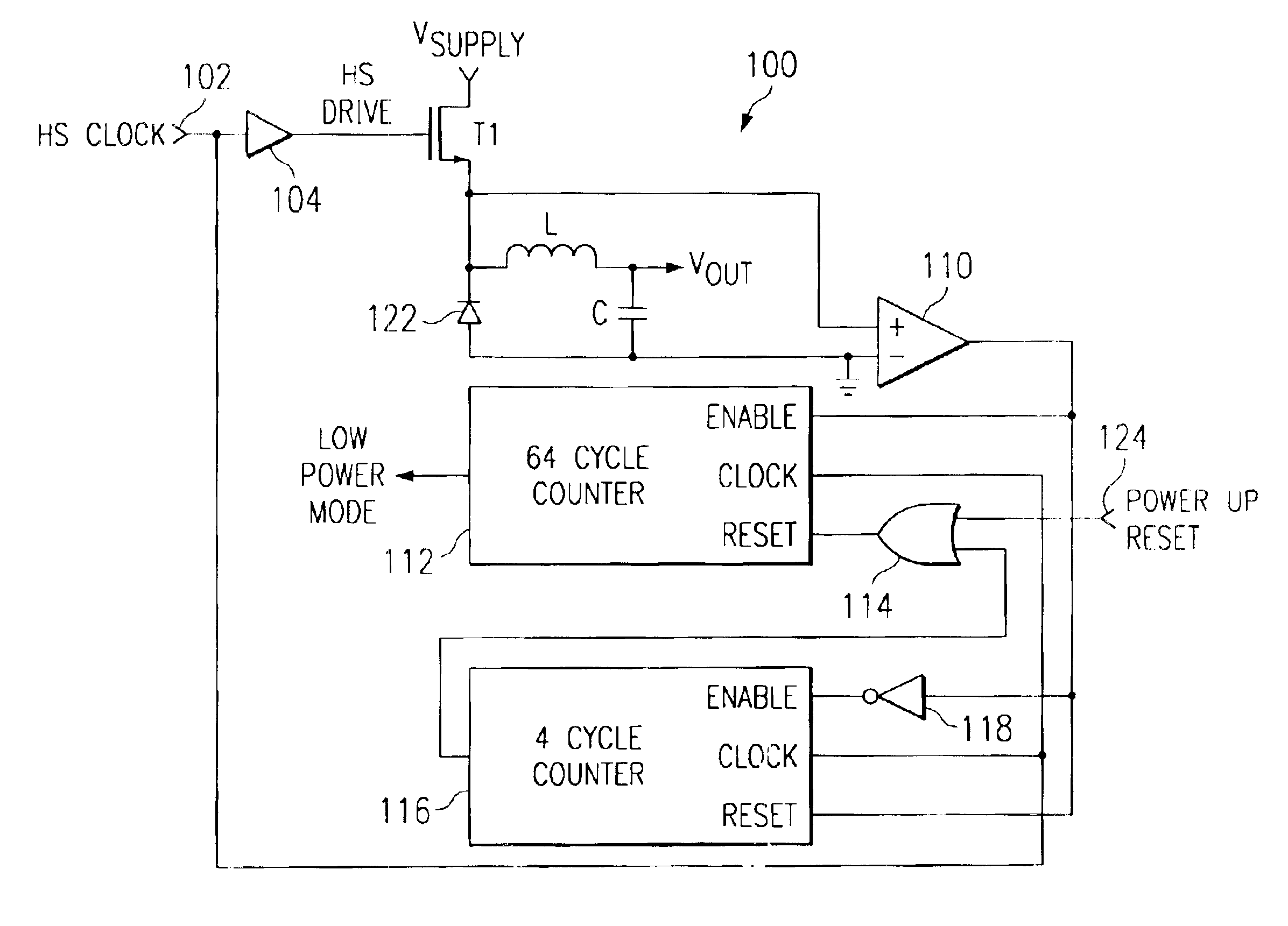
Referring to FIG. 1, a schematic block diagram of a buck DC / DC is generally shown as 100. The switching regulator 100 utilizes a conventional configuration including a first switching transistor T1 coupled between a power Vsupply and a reverse biased diode 122 to ground. An inductor L has a first terminal coupled to the node between the switching transistor T1 and the diode 122 and having a second terminal which is the output voltage of the switching regulator. A capacitor C is coupled between the second terminal of the inductor L and ground. The switching transistor T1 is driven by a clock signal labeled HS clock at terminal 102 and a driver 104. The output of the driver 104 is labeled as the signal HS drive. Not illustrated in the drawing for simplicity in illustration and to enhance the understanding of the present invention, is a feedback circuit from the output of the regulator to control the switching of transistor T1 in order to regulate the output voltage. These feedback con...


PUM


Abstract

A DC/DC converter has a semiconductor switch coupled to an inductor, a capacitor and a rectifier. A comparator is coupled to across the rectifier to detect a polarity reversal during the second portion of converter operation to place the converter in a low power mode if the voltage across the rectifier is of an appropriate polarity for reverse current flow. The rectifier may be a synchronous rectifier transistor and the voltage converter placed in a low power mode when the polarity across the synchronous rectifier indicates that reverse current flow is possible. A timing circuit delays the generation of the control signal to place the converter in a low power mode until the steady state current is below a predetermined threshold for a predetermined amount of time. The synchronous rectifier may be turned OFF when the current through the converter falls below another predetermined threshold value and the voltage across the synchronous rectifier will become the voltage across the parasitic diode of the FET synchronous rectifier.

Description

FIELD OF THE INVENTIONThis invention relates to a DC / DC switching regulator and more specifically to a DC / DC switching regulator for an automobile instrument cluster.BACKGROUND OF THE INVENTIONDC / DC switching regulators or converters are part of many power management systems because of the improved power conversion efficiency provided by these regulators over that of linear regulators. Switching regulator designs can achieve efficiencies as high as 90% or more where as the efficiency of linear regulators is dependent strictly upon the difference between the input voltage and the output voltage. DC / DC switching regulators can take the form of a buck or voltage reducing regulator, a boost converter, which increases the input voltage, or a buck / boost converter, which can perform both functions.It has now become common place for active loads to enter reduced power or “sleep” modes in which portions of the circuit not currently necessary for operation are shut off in order to conserve po...

Claims


Application Information

Patent Timeline
Patent Type & Authority Patents(United States)
IPC IPC(8): H02M3/158H02M3/04H02M3/156
CPCH02M3/156H02M3/1588Y02B70/16Y02B70/1466H02M2001/0032Y02B70/10H02M1/0032
Inventor BALDWIN, DAVID J.KOHOUT, JAMES A.
Owner TEXAS INSTR INC
Why Eureka
Try Eureka