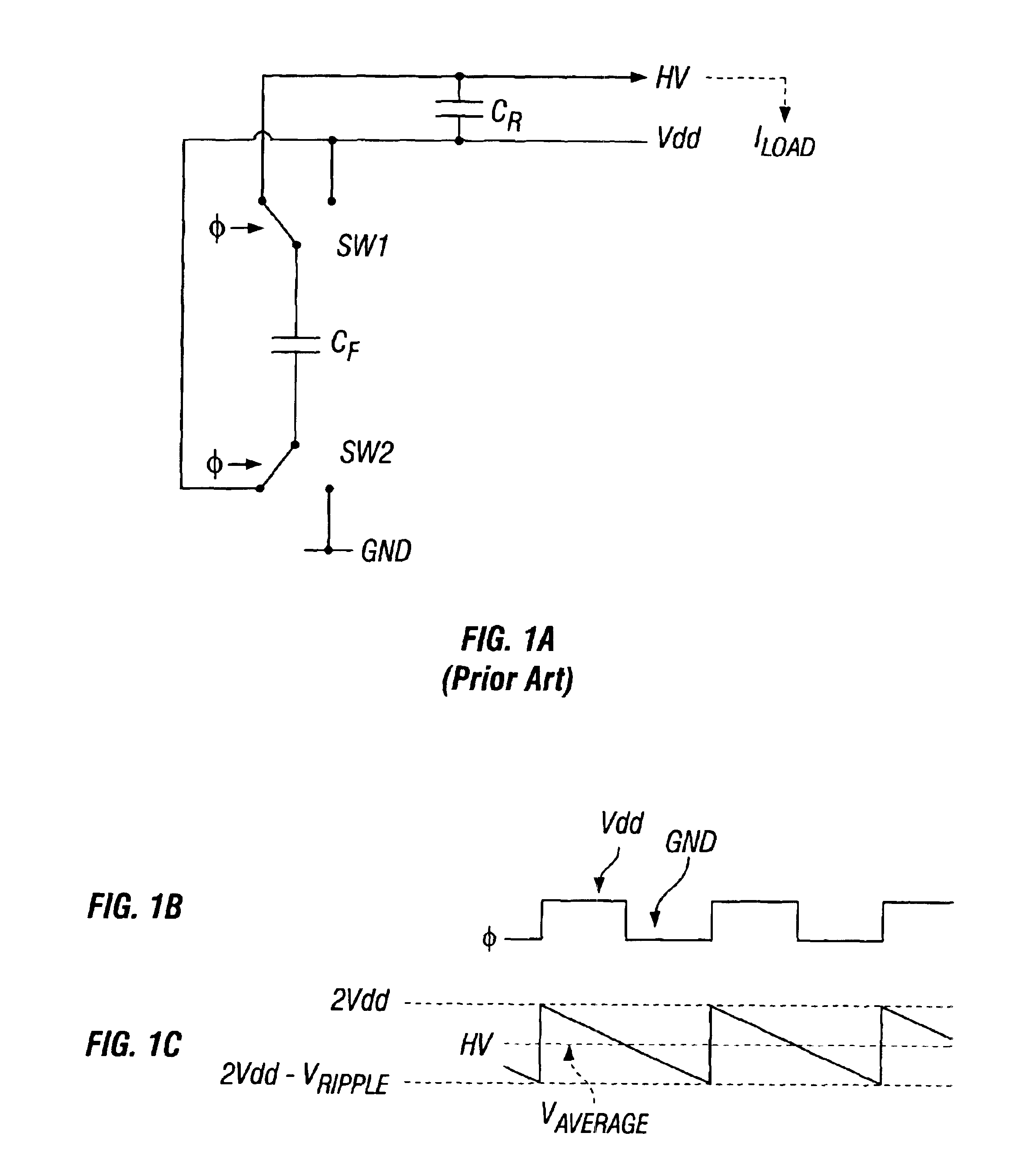
1. For a given load current, increasing the size of the
reservoir capacitor CR proportionally decreases the
ripple, but also proportionally increases both the area (CR is generally by far the largest component in such a charge pump) and the turn-on time (number of cycles of Φ required to initially charge node HV to its target
voltage of 2Vdd).
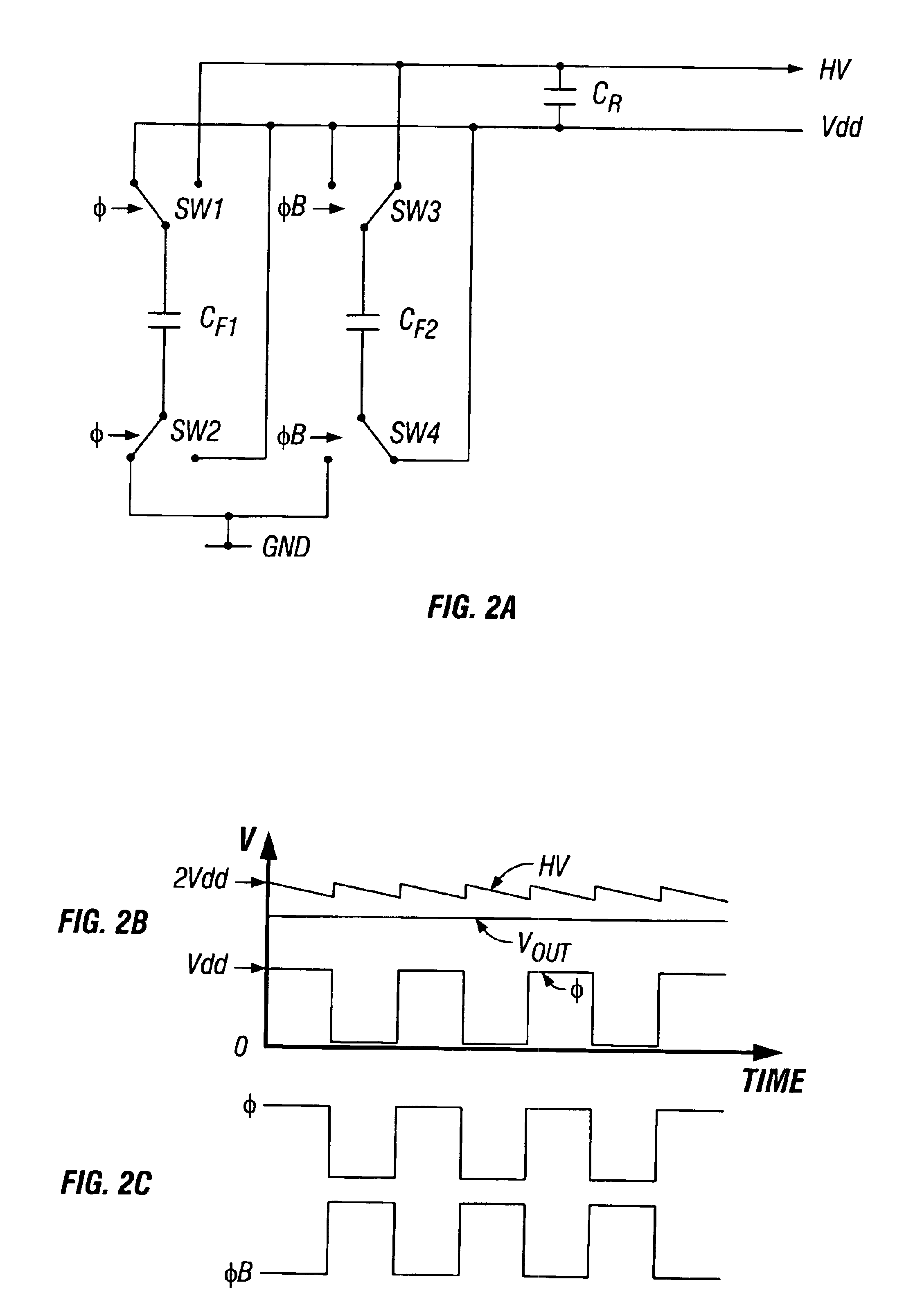
2. It is very common to attempt to provide a more continuous supply of charge from the flying
capacitor. This can be achieved for instance, as shown in FIG. 2a, by splitting the flying
capacitor into two devices with switches SW1 through SW4 driven by
clock phases 180 degrees apart (depicted as Φ and ΦB in FIG. 2c). Still the output HV contains substantial
ripple, as shown in FIG. 2b. Clearly, if capacitor CF were split into an
infinite number of devices driven by an infinite set of clocks
phase shifted from Φ by 0° to 360°, then the
ripple would be zero. However, note that as the number of flying capacitors is increased, so does the number of switches. Complexity in the
clock generation circuits and the inefficiency introduced by manipulating the switches prevents more than a very few phase-shifted flying capacitors being used.
This immediately introduces significant inefficiency in the
pump design.
As breakdown voltages are becoming smaller and smaller with decreasing process geometries, this can be a significant
disadvantage.
1. Continuous frequency, amplitude =Vdd. In this scheme (the simplest scheme), if the load current is constant, an average
voltage will result at node HV such that the average charge removed from the capacitor CR by the load in time Δt is equal to the average charge supplied by the flying capacitors CF1 and CF2 in the same time period Δt. This is an open loop system. If the load current changes, the output voltage at node HV responds to compensate and keep the above equality true. Therefore, higher load currents reduce the voltage at HV, lower load currents increase it. Similarly, changes in the supply voltage Vdd directly affect the achieved output voltage. For varying loads, this is a very inefficient approach, yet is very common (see Dickson, IEEE Journal of
Solid State Circuits, Vol SC-11, No. 3, June 1976, pp 374-378). Often, a voltage sensitive
current clamp (e.g.
zener diode) is used to regulate the output of such a charge pump by dumping the excess current supplied by the charge pump, resulting in a very low efficiency.
2. Continuous frequency, amplitude <Vdd. In this scheme, a reference voltage is used instead of Vdd to ensure that the amplitude of the clocking
signal is independent of Vdd. This ensures that the output voltage at node HV is independent of supply voltage variations, but it is still sensitive to load current variations as described in technique 1 above.
3. Continuous frequency, variable amplitude. Here, an indicative circuit parameter is monitored and the amplitude of the clocking waveforms modulated accordingly to maintain a
constant voltage at node HV. Typically, the voltage on node HV is monitored itself (see U.S. Pat. No. 6,300,820), although other parameters can be observed (see U.S. Pat. No. 6,002,630).
4. Variable frequency, fixed amplitude. Here, an indicative circuit parameter is monitored and the frequency of the clocking waveforms modulated accordingly to maintain a
constant voltage at node HV. Typically, once again, the voltage on node HV is monitored (see U.S. Pat. Nos. 6,115,272 and 6,310,789,).
5. Variable frequency, variable amplitude. Techniques 3 and 4 above can be combined, as demonstrated in U.S. Pat. No. 6,188,590.

