Memory array of a non-volatile ram

a non-volatile, memory array technology, applied in the field of memory, can solve the problems of resistance-changing properties of certain cmos, which have not yet been implemented in a commercially viable memory produ

Inactive Publication Date: 2005-02-22
UNITY SEMICON
View PDF9 Cites 134 Cited by
  • Summary
  • Abstract
  • Description
  • Claims
  • Application Information

AI Technical Summary

Benefits of technology

The semiconductor device controls current flow between the data line and the reference line depending on the voltage of the select line. Located between the data line and the reference line is the multi-resistive state material, which changes its resistive state from a high resistive state to a low resistive state upon application of a first voltage pulse across the multi-resistive state material and changes its resistive state from the low resistive state to the high resistive state upon application of a second voltage pulse across the multi-resistive state material. The second voltage pulse across the multi-resistive state material is of opposite polarity to the first voltage pulse.
It is the resistive state of the multi-resistive state material that determines the information stored in the memory cell. In the first aspect of the invention, at least one intermediary resistive state is used so that the memory cell is capable of storing more than one bit of information, whereby the multi-resistive state material is placed i...

Problems solved by technology

However, the materials described in the U.S. Pat. No. 6,204,139 patent is not generally applicable to RAM memory because the resistance of the material, when scaled to small dimensions, is considered to be too ...

Method used


Image

  • Memory array of a non-volatile ram
  • Memory array of a non-volatile ram
  • Memory array of a non-volatile ram

Examples


Embodiment Construction

In the following description, numerous specific details are set forth to provide a thorough understanding of the present invention. It will be apparent, however, to one skilled in the art that the present invention may be practiced without some or all of these specific details. In other instances, well known process steps have not been described in detail in order to avoid unnecessarily obscuring the present invention.

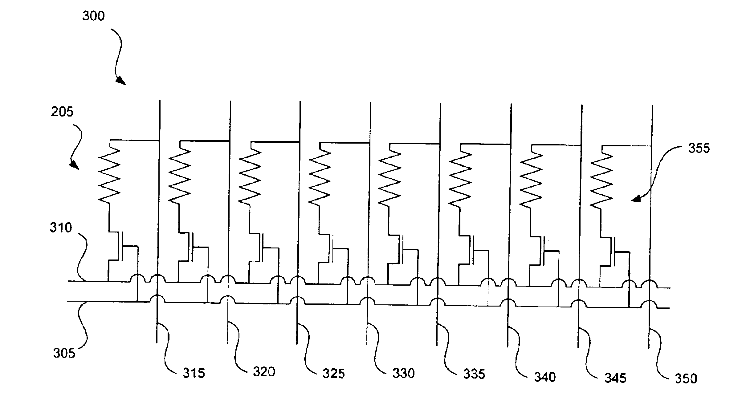
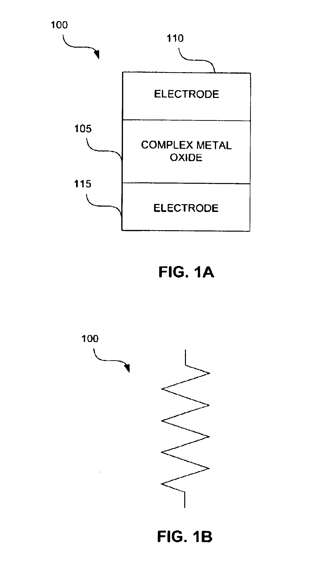
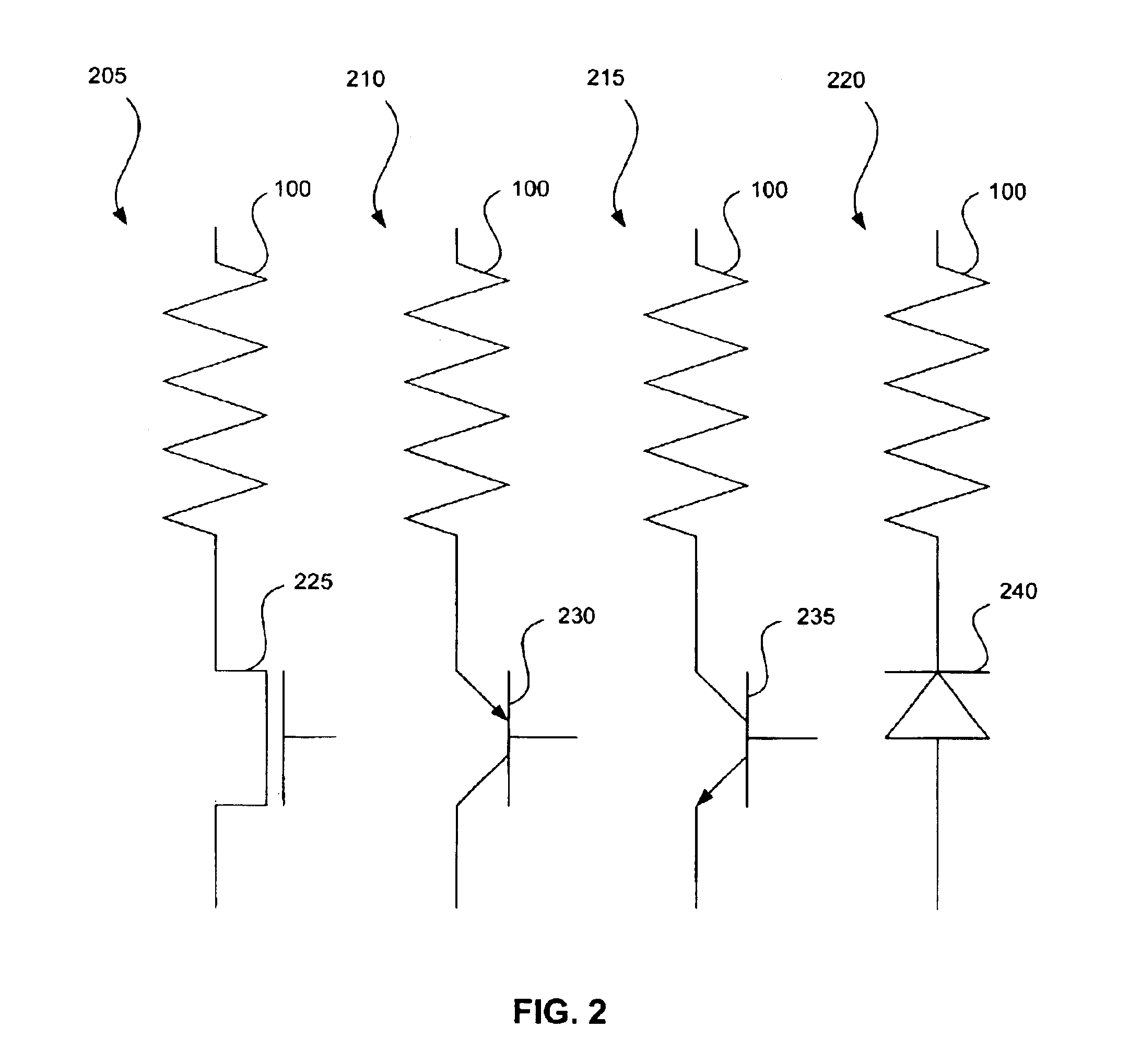
The present invention generally allows for multi-resistive state materials to be used as memory elements in a non-volatile RAM memory. Multi-resistive state materials generally require high temperature processing, which limits the types of material that can be used prior to the multi-resistive state material deposition. A non-volatile RAM chip that only uses materials that can withstand the high temperature processing below the multi-resistive state material is free to use regular materials above the multi-resistive state material, since those materials are not subject...


PUM


Abstract

Non-volatile memory cell with a single semiconductor device per memory cell. The present invention generally allows for a plurality of memory cells to be formed on a semiconductor substrate that supports a semiconductor device. A multi-resistive state material layer that changes its resistive state between a low resistive state and a high resistive state upon application of a voltage pulse is formed above the substrate, generally at a very high temperature. While the layers fabricated between the substrate and the multi-resistive state material use materials that can withstand high temperature processing, the layers fabricated above the multi-resistive state material do not need to withstand high temperature processing.

Description

BACKGROUND OF INVENTION1. Field of the InventionThe present invention relates generally to memory, and more specifically to memory that uses multi-resistive state materials as resistive memory elements.2. Description of the Related ArtMemory can either be classified as volatile or nonvolatile. Volatile memory is memory that loses its contents when the power is turned off. Some solid-state memory devices do not require a continuous power supply to retain information.Certain complex metal oxides (CMOs), for example, can retain a resistive state after being exposed to an electronic pulse, which can be generated from two terminals. U.S. Pat. No. 6,204,139, issued Mar. 20, 2001 to Liu et al., incorporated herein by reference for all purposes, describes some perovskite materials that exhibit such characteristics. The perovskite materials are also described by the same researchers in “Electric-pulse-induced reversible resistance change effect in magnetoresistive films, “Applied Physics Let...

Claims


Application Information

Patent Timeline
IPC IPC(8): G11C11/56G11C13/00G11C16/02H01L21/8246H01L27/115H01L27/24H01L45/00
CPCG11C11/5678H01L45/1675G11C13/0007H01L27/11502H01L27/11507H01L27/2436H01L45/04H01L45/10H01L45/1233H01L45/147H01L45/1608H01L45/1616H01L45/1625H01L45/1641G11C11/5685G11C13/0004G11C2213/31G11C2213/79H01L27/2409H01L27/2445H10B63/32H10B63/20H10B63/30H10N70/20H10N70/826H10N70/8836H10N70/021H10N70/026H10N70/023H10N70/041H10N70/063H10B53/30H10B53/00
Inventor RINERSON, DARRELLCHEVALLIER, CHRISTOPHE J.
Owner UNITY SEMICON
Why Eureka
Try Eureka