Fully-hidden refresh dynamic random access memory

a dynamic random access memory and fully hidden technology, applied in the field of fully hidden refresh dram (dynamic), can solve the problems of data destruction, sizing of the entire system, and inability to ensure the correct data access operation

Inactive Publication Date: 2005-02-22
RENESAS ELECTRONICS CORP
View PDF14 Cites 22 Cited by
  • Summary
  • Abstract
  • Description
  • Claims
  • Application Information

AI Technical Summary

Benefits of technology

[0016]It is an object of the present invention to provide a fully hidden refresh DRAM capable of performing a correct data access regardless of a timing of application of an external data access instruction with respect to an internal operating state.

Problems solved by technology

The DRAM, however, stores information in a capacitor in the form of electric charges and electric charges accumulated in the capacitor leak out over time to cause destruction of data.
If such a large capacity memory device is constructed using an SRAM, an occupation area of the memory would be increased, to be a great obstacle against down-sizing of the entire system.
The refresh timer operates asynchronously with external data access, and a necessity arises for arbitration between a refresh request and a data access instruction since data destruction occurs when an external data access and a refresh request conflict with each other.
Therefore, there is a possibility that the data access operation is started before an internal circuit does not restore completely to a prescribed initial state, and correct data access operation could not ensured.
If a refresh request is issued when a normal data access request is deactivated and a precharge operation is being internally performed, a similar problem arises.
Therefore, such a prior art technique has a problem that it can not be applied to an interface utilizing an address transition detection signal generally widely adapted as an interface of the SRAM.
Therefore, the prior art technique could not accommodate for an interface of an address transition detection type, thereby disabling implementation of a DRAM having complete compatibility with an SRAM.
In a case where the next data access instruction is supplied before the prescribed time elapses, the next data access operation is performed prior to restoration of internal circuitry to a precharged state, data collision may occur to cause a problem of correct data access being not ensured.

Method used


Image

  • Fully-hidden refresh dynamic random access memory
  • Fully-hidden refresh dynamic random access memory
  • Fully-hidden refresh dynamic random access memory

Examples


sixth embodiment

[0053]FIG. 30 is a timing chart representing an operation of the semiconductor memory device according to the present invention;

seventh embodiment

[0054]FIG. 31 is a diagram schematically showing a configuration of a main part of a semiconductor memory device according to the present invention;

[0055]FIG. 32 is a timing chart representing an operation of the circuitry shown in FIG. 31;

eighth embodiment

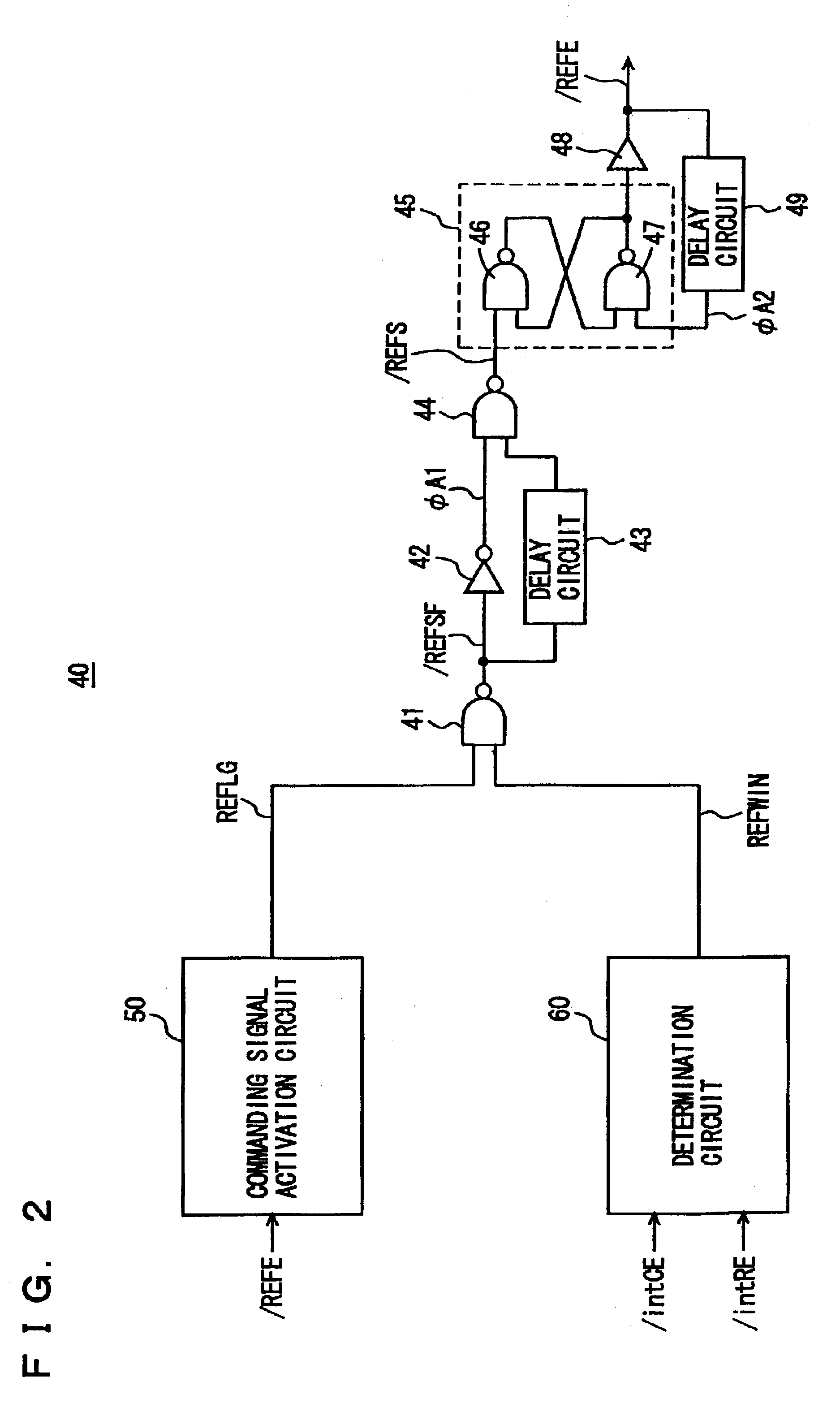
[0056]FIG. 33 is a diagram schematically showing a configuration of a main part of a semiconductor memory device according to the present invention;

[0057]FIG. 34 is a timing chart representing an operation of the determination circuit shown in FIG. 33;

[0058]FIG. 35 is a timing chart representing an operation of the circuitry shown in FIG. 34; and

[0059]FIG. 36 is a timing chart representing an operation in a short cycle of the semiconductor memory device shown in FIG. 33.

DESCRIPTION OF THE PREFERRED EMBODIMENTS


PUM


Abstract

A composite gate detects whether an internal array is in a selected state and an internal row activation signal is activated in accordance with a timing relationship between an output signal of the composite gate and an address transition detection signal. When the address transition detection signal is applied, the internal row activation signal is deactivated in accordance with generation timings of delayed restore period signal indicating whether the internal array is in a selected state and of the address transition detection signal to permit the next row access. With such a configuration, the next operation is allowed to start after an internal state is surely restored to an initial state. When the next address transition detection signal is applied during a period of a restoration operation, a column recovery operation, or a refreshing operation, data access is correctly performed without causing data destruction.

Description

BACKGROUND OF THE INVENTION[0002]1. Field of the Invention[0003]The present invention relates to a semiconductor memory device, and particularly to a fully-hidden refresh DRAM (Dynamic Random Access Memory) capable of fully hiding an internally performed refreshing operation from an outside. More particularly, the present invention relates to a dynamic semiconductor memory device having an interface fully compatible with an SRAM (Static Random Access Memory).[0004]2. Description of the Background Art[0005]A DRAM (Dynamic Random Access Memory) is in general constructed from memory cells each constituted of one transistor and one capacitor. Therefore, an occupation area of the memory cell is small and DRAM is suited for implementation of a large capacity memory device. The DRAM, however, stores information in a capacitor in the form of electric charges and electric charges accumulated in the capacitor leak out over time to cause destruction of data. Therefore, in order to prevent the ...

Claims


Application Information

Patent Timeline
Patent Type & Authority Patents(United States)
IPC IPC(8): G11C11/406G11C11/403
CPCG11C8/18G11C11/40615G11C11/40603G11C11/406
Inventor TAKATSUKA, TAKAFUMISATO, HIROTOSHITSUKUDE, MASAKI
Owner RENESAS ELECTRONICS CORP
Why Eureka
Try Eureka