Self assembled micro anti-stiction structure

Inactive Publication Date: 2005-02-22
ANALOG DEVICES INC
View PDF16 Cites 20 Cited by
  • Summary
  • Abstract
  • Description
  • Claims
  • Application Information

AI Technical Summary

Benefits of technology

The disadvantages associated with the prior art are overcome by embodiments of the present the present invention directed to a method and apparatus for reducing stiction in a MEMS device having a movable element and a substrate. The method generally comprises providing the substrate with an anti-stiction member and interposing the anti-stiction member between the moveable element and the substrate. The apparatus generally comprises an anti-stiction member that is interposable between the moveable element and the substrate. Another embodiment of the invention of the invention is directed to a MEMS device, comprising: a substrate, a moveable element moveably coupled to the substrate, and an anti-stiction member that is interposable between the moveable element and the substrate. A further embodiment of the invention is directed to an optical switch. The optical switch generally includes a substra

Problems solved by technology

In addition, stiction forces can also prevent the mirror from being properly released from the substrate during manufacture.
However, such standoffs are difficult to fabricate, particularly when they are to be fabricated from the device layer of an SOI substrate.
Con

Method used


Image

  • Self assembled micro anti-stiction structure
  • Self assembled micro anti-stiction structure
  • Self assembled micro anti-stiction structure

Examples


Embodiment Construction

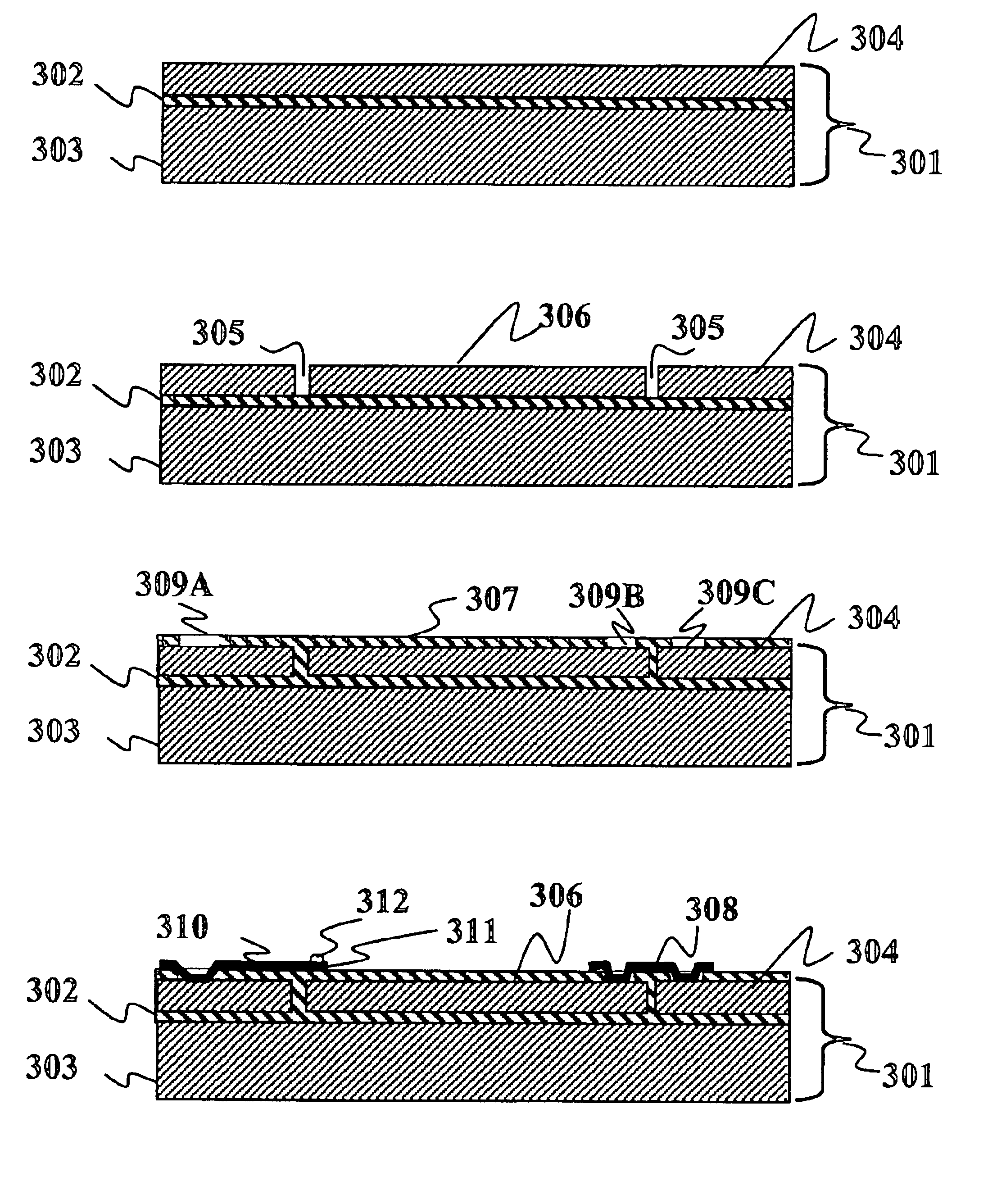
This invention proposes a different method to reduce the contact area by building a novel structure that self-assembled. The approach of the present invention may complement other methods to more effectively eliminate stiction. This method is particularly suitable for (but is not limited to) devices built on SOI wafers. Although the following detailed description contains many specific details for the purposes of illustration, anyone of ordinary skill in the art will appreciate that many variations and alterations to the following details are within the scope of the invention. Accordingly, the examples of embodiments of the invention described below are set forth without any loss of generality to, and without imposing limitations upon, the claimed invention.

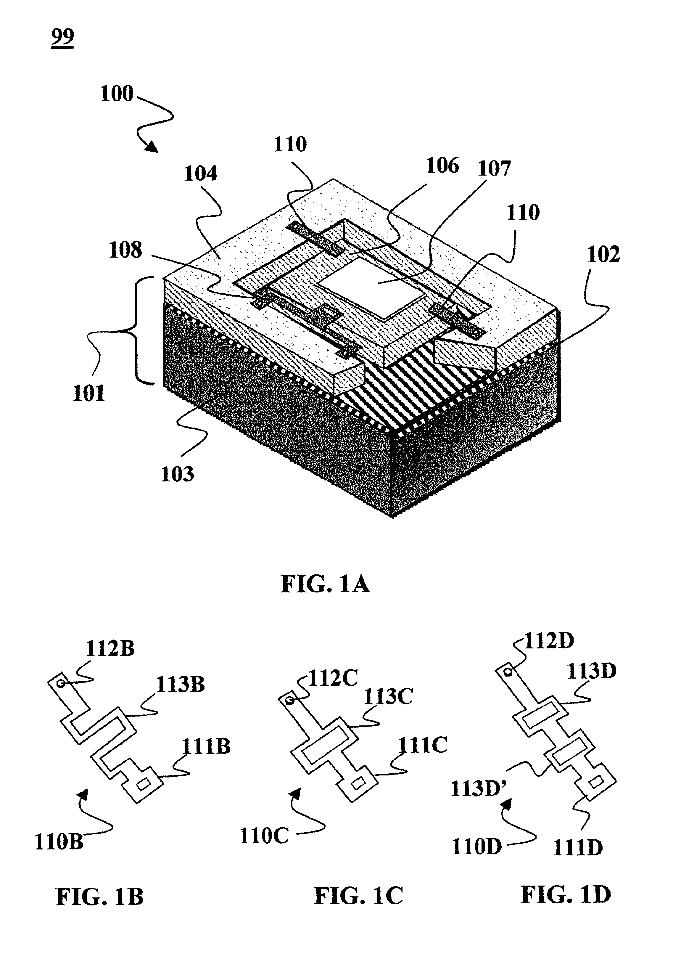
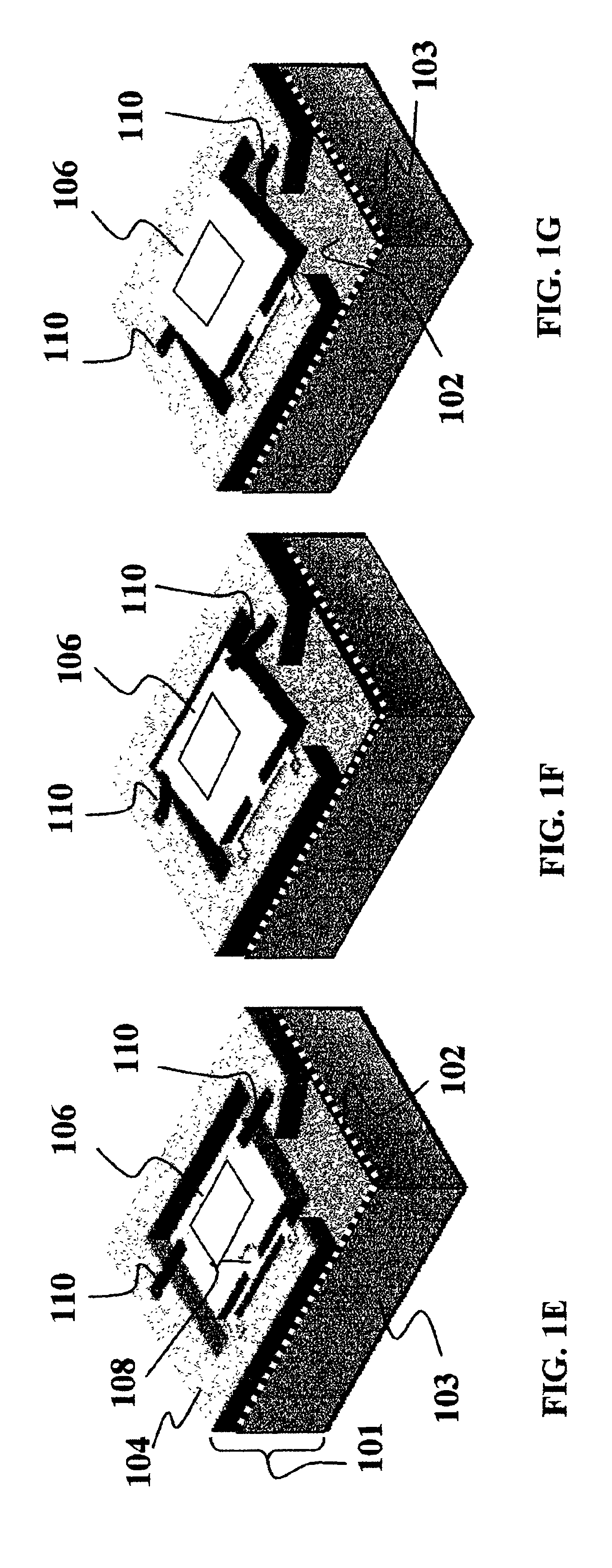
FIG. 1A depicts an example of an apparatus 99 for reducing stiction according to an embodiment of the present invention. The apparatus 99 generally includes a MEMS device 100 having a moveable element 106 moveably coupled to a su...


PUM

PropertyMeasurementUnit
Flexibilityaaaaaaaaaa
aaaaaaaaaa

Abstract

A method and apparatus are described for reducing stiction in a MEMS device having a movable element and a substrate. The method generally comprises providing the substrate with an anti-stiction member and interposing the anti-stiction member between the moveable element and the substrate. The apparatus generally comprises an anti-stiction member that is interposable between the moveable element and the substrate. Another embodiment of the invention of the invention is directed to a MEMS device, comprising: a substrate, a moveable element moveably coupled to the substrate, and an anti-stiction member that is interposable between the moveable element and the substrate. A further embodiment of the invention is directed to an optical switch having one or more moveable elements moveably coupled to a substrate, and an anti-stiction member that is interposable between at least one of the moveable elements and the substrate. The anti-stiction member may be in the form of a flexible cantilevered structure that overhangs the moveable element. Actuating the moveable element causes the anti-stiction member to flex and snap into place between the moveable element and the substrate. An additional embodiment of the invention is directed to a method of fabricating a MEMS device. The method proceeds by providing a silicon-on-insulator (SOI) substrate; defining a moveable element from a device layer of the SOI substrate; and depositing a flexible material over the device layer and the moveable element. One or more portions of the flexible material overhang the moveable element, whereby the flexible material forms one or more anti-stiction members.

Description

FIELD OF THE INVENTIONThis invention relates generally to microelectromechanical structures (MEMS). More particularly, it relates to reducing stiction in MEMS devices such as those used in optical switches.BACKGROUND OF THE INVENTIONMicroelectromechanical systems (MEMS) are miniature mechanical devices manufactured using the techniques developed by the semiconductor industry for integrated circuit fabrication. Such techniques generally involve depositing layers of material that form the device, selectively etching features in the layer to shape the device and removing certain layers, known as sacrificial layers, to release the device. Such techniques have been used, for example, to fabricate miniature electric motors as described in U.S. Pat. No. 5,043,043.Silicon-on-insulator (SOI) techniques have been developed for fabricating MEMS devices. In SOI, an oxide layer is grown or deposited on a silicon wafer. A second silicon wafer is then bonded to the oxide layer, e.g. by fusion bond...

Claims


Application Information

Patent Timeline
IPC IPC(8): G02B26/08B81B3/00
CPCB81B3/0008G02B26/0841B81B2203/058B81B2201/045
Inventor LIN, CHUANG-CHIA
Owner ANALOG DEVICES INC
Why Eureka
Try Eureka