
Data processing system

a data processing system and data processing technology, applied in the field of data processing systems, can solve the problems of limiting the affecting the performance of the system, and affecting the efficiency of the system, so as to achieve the effect of wide scalable parallelity, fast and flexible, and greater, or better, flexibility of the overall structur

Inactive Publication Date: 2005-02-22
PACT XPP TECH
View PDF136 Cites 79 Cited by
  • Summary
  • Abstract
  • Description
  • Claims
  • Application Information

AI Technical Summary

Benefits of technology

An additional advantage of the present invention is that a widely scalable parallelity is available. Created here is a basis for a fast and flexible creation of neuronal structures such as to date can be simulated only at considerable expense.
is that a widely scalable parallelity is available. Created here is a basis for a fast and flexible creation of neuronal structures such as to date can be simulated only at considerable expense.
The objective underlying the present invention is to propose a data processing system which hereafter will be referred to as data flow processor (DFP), where a greater, or better, flexibility of the overall structure and data flow as well as pipelining and cascading options result in increased processor capacity, or linking capacity.
Besides its employment as strictly a data flow processor, the DFP is meant to be able to handle the following further tasks:utilization as universal module in setting up conventional computers, making the structure simpler and less expensive;utilization in neuronal networks.
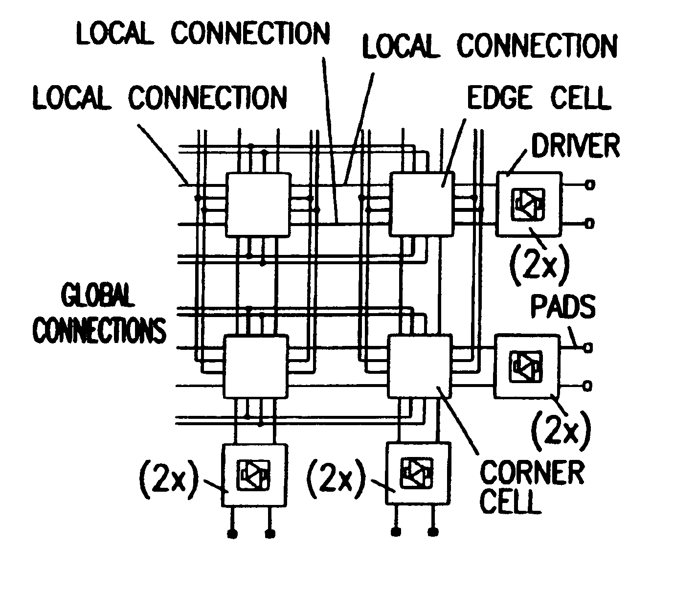
This objective is accomplished by providing an integrated circuit (chip) with a plurality of cells which, in particular, are arranged orthogonally to one another, each with a plurality of logically same and structurally identically arranged cells, whose arrangement and internal bus structure is extremely homogeneous so as to facilitate programming. Nonetheless, it is conceivable to accommodate within a data flow processor cells with different cell logics and cell structures in order to increase the capacity in that, for example, there exist for memory access other cells than for arithmetic operations. A certain specialization can be advantageous, especially for neuronal networks. Coordinated with the cells is a loading logic by way of which the cells, by themselves and facultatively grouped in so-called MACROs, are so programmed that, for one, selective logical functions but, for another, also the linking of cells among themselves can be realized widely. This is achieved in that for each individual cell a certain memory location is available in which the configuration data are filed. These data are used to switch multiplexers or transistors in the cell so as to guarantee the respective cell function (refer to FIG. 12).
The core of the present invention consists in proposing a data flow processor of cellular structure whose cells allows reconfiguration in an arithmetic-logical sense, quasi randomly, via an external loading logic. Of extreme necessity is that the respective cells allow reconfiguration individually and without affecting the remaining cells or disabling the entire module. Thus, the data flow processor according to the present invention can be “programmed” as an adder in a first operating cycle and as a multiplier in a subsequent operating cycle, wherein the number of cells required for addition or multiplication may well be different and the placement of already loaded MACROs is upheld. It is incumbent upon the loading logic, or compiler, to partition the newly loaded MACRO within the available cells (i.e., to dissect said MACRO in such a way that it allows optimum insertion). The sequence control of the program is assumed by the compiler, which loads the appropriate MACROs in the module in accordance with the presently performed program section, the loading process being concomitantly controlled by the yet to be described synchronization logic, which determines the moment of reloading. Therefore, the DFP does not Correspond to the known von Neumann architecture, since the data and program memories are separate. But this means at the same time increased security, since faulty programs cannot destroy a CODE, but merely DATA.

Problems solved by technology

Also, it is readily evident that the hardware structure of the arithmetic-logic linking unit cannot be considered as optimal inasmuch as the integrated logic hardware modules are actively used within the overall system always only in one and the same way.
Similarly, a compilation of functions in so-called pipelines is very much impeded or restricted by strict hardware specification, which of necessity means frequent register reloading between working registers and central processing unit.
Furthermore, such modules lend themselves poorly to cascading and require then substantial programming work.

Method used


Image

  • Data processing system
  • Data processing system
  • Data processing system

Examples


Embodiment Construction

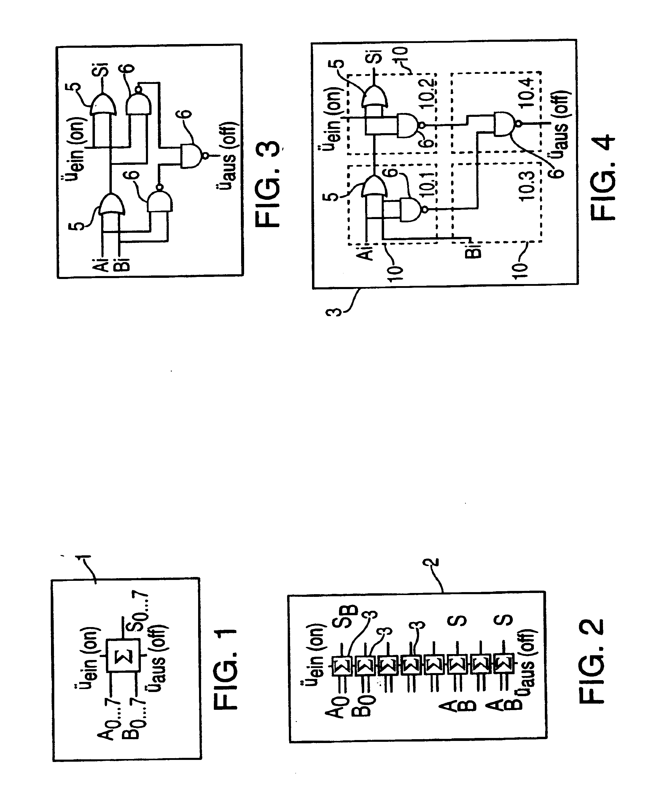
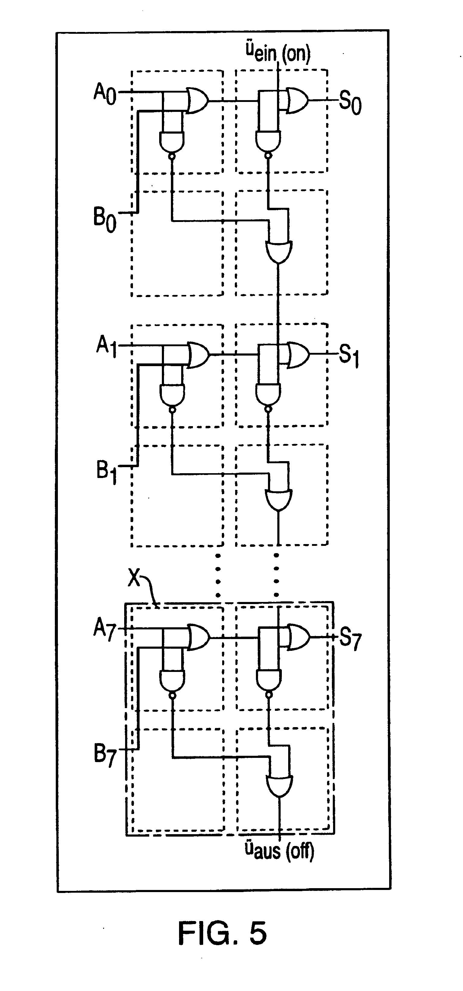
FIG. 1 illustrates a circuitry symbol for an 8-bit adder. Said wiring symbol consists of a quadratic module 1 with eight inputs A 0 . . . 7 for a first data word A and eight inputs B 0 . . . 7 for a second data word B (to be added). The eight inputs Ai, Bi are supplemented each by a further input Üein, by way of which, as the case may be, a carry-over is passed on to the module 1. In keeping with its function and purpose, the module 1 has eight outputs S 0 . . . 7 for binary summands and a further output Üaus for any existing carry-over.

The circuitry symbol illustrated in FIG. 1 is shown in FIG. 2 as an arrangement of so-called SUBMACROs. Said SUBMACROs 2 consist each of a 1-bit adder 3 with one input each for the appropriate bits of the data word and a further input for a carry-over bit. Furthermore, the 1-bit adders 3 feature an output for the summand and an output for the carry-over Üaus.

Shown in FIG. 3 is the binary logic of a 1-bit adder, or SUBMACRO 2 according to FIG. 2. Anal...


PUM


Abstract

A data processing system, wherein a data flow processor (DFP) integrated circuit chip is provided which comprises a plurality of orthogonally arranged homogeneously structured cells, each cell having a plurality of logically same and structurally identically arranged modules. The cells are combined and facultatively grouped using lines and columns and connected to the input / output ports of the DFP. A compiler programs and configures the cells, each by itself and facultatively-grouped, such that random logic functions and / or linkages among the cells can be realized. The manipulation of the DFP configuration is performed during DFP operation such that modification of function parts (MACROs) of the DFP can take place without requiring other function parts to be deactivated or being impaired.

Description

BACKGROUND OF THE INVENTIONThe present invention relates to a data processing system, i.e., a hardware unit for logical manipulation (linkage) of data (information) available in binary form.Data processing systems of this type have by now been known long since, and they have already found broad application and recognition. The basic structure and operation of prior data processing systems can be defined approximately as comprising an arithmetic-logic linking unit in which the data to be linked are processed according to program instructions (software). In the process, the data are retrieved appropriately via a controller by more or less complex addressing procedures and, to begin with, kept ready in working registers. Following the logical linkage, the new data are then filed again in a preset memory location. The arithmetic-logic linkage unit consists of logical linking modules (gates, members) that are coupled to one another in such a way that the data to be manipulated allows in ...

Claims


Application Information

Patent Timeline
IPC IPC(8): G06F13/00G06F17/00G06F15/00
CPCG06F15/7867G06F2213/0038
Inventor VORBACH, MARTIN
Owner PACT XPP TECH
Learn More