Low-pin-count chip package and manufacturing method thereof

Inactive Publication Date: 2005-03-01
ADVANCED SEMICON ENG INC
View PDF12 Cites 52 Cited by
  • Summary
  • Abstract
  • Description
  • Claims
  • Application Information

AI Technical Summary

Benefits of technology

Accordingly, in a first aspect, the present invention provides a low-pin-count chip package including a die pad for receiving a semiconductor chip and a plurality of connection pads electrically coupled to the semiconductor chip. A package body is formed over the semiconductor chip and the connection pads in a manner that the lower surfaces of the die p

Problems solved by technology

Because of the CTE mismatch, stresses are induced at the interface between the connection pads and the plastic package body as the conventional package experiences temperature cycling.
Once moisture accumulates in the package, rapid temperature ramp-up will cause the moisture to vaporize and expand, thereby inducing an hygrothermal stresses in the delaminated area which caus

Method used


Image

  • Low-pin-count chip package and manufacturing method thereof
  • Low-pin-count chip package and manufacturing method thereof
  • Low-pin-count chip package and manufacturing method thereof

Examples


first embodiment

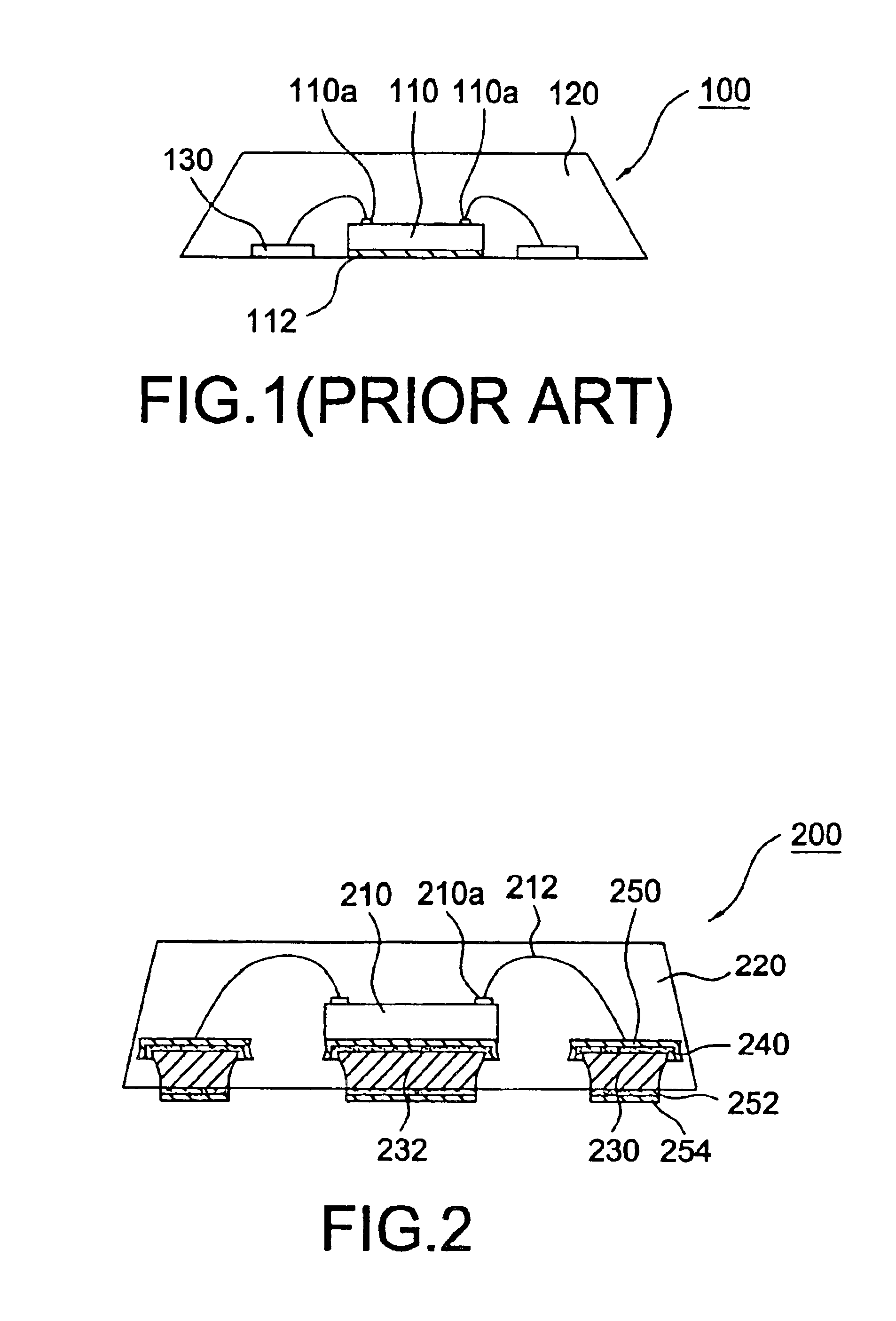
FIG. 2 discloses a low-pin-count chip package 200 in accordance with the present invention comprising a chip 210 attached to a die pad 232 by either a conductive adhesive layer or nonconductive adhesive layer, e.g., epoxy (not shown). The active surface of the chip 210 is provided with a plurality of bonding pads 210a electrically connected to connection pads 230 through bonding wires 212. The connection pads 230 are arranged at the periphery of the die pad 232. The connection pads 230 and the die pad 232 are exposed from the bottom of the package body 220 and both of them have a substantially tapering profile for enhancing the “locking” of the die pad 230 and the connection pads 232 into predetermined place in the package body 220 as well as prolonging the path and time for moisture diffusion into the package 200. A package body 220 is formed over the semiconductor chip 210 and the connection pads 230.

Preferably, the die pad 232 and the connection pads 230 are provided with a metal...

second embodiment

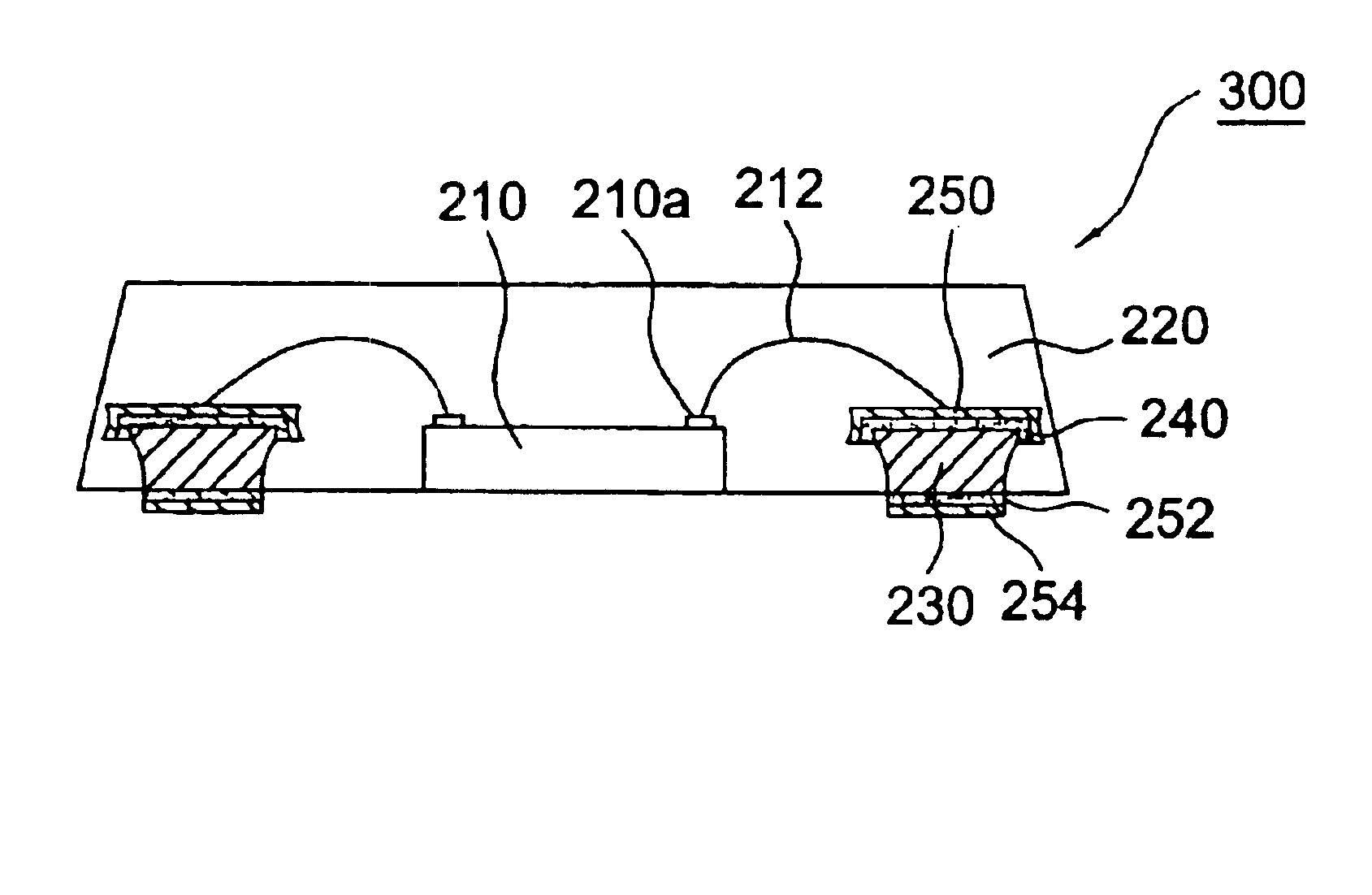
FIG. 11 discloses a low-pin-count chip package 300 in accordance with the present invention comprising a chip 210 sealed in a package body 220. The chip package 300 is substantially identical to the chip package 200 of FIG. 2 with exception that the die pad 232 is skipped and the adhesive layer (not shown) is directly exposed from the package body 220.

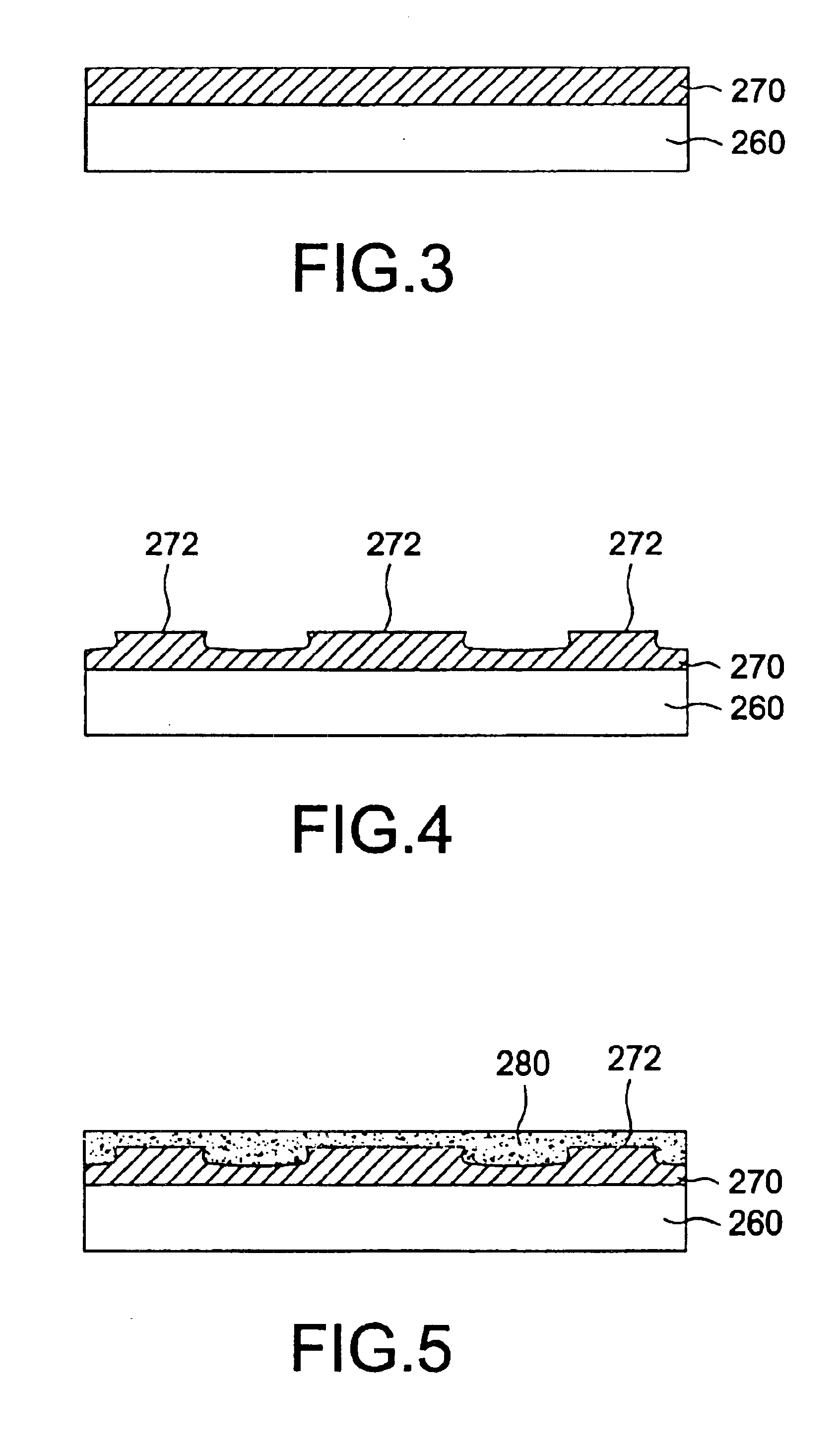
FIGS. 12-15 illustrate a method of making the low-pin-count chip package 300 according to a second embodiment of the present invention.

Referring to FIG. 12, a metal layer 270 is laminated on a sheet carrier 260 and the metal layer 270 is half-etched to form concavities at predetermined positions thereof. Projections 272 not etched in the half-etching process will form the connection pads 230 afterward.

Referring to FIG. 13, a photoresist layer 280 is formed on the metal layer 270 and half-removed such that only photoresist within the concavities is left. It is noted that projections 272 are substantially exposed from the remaining photo...


PUM


Abstract

A low-pin-count chip package including a die pad for receiving a semiconductor chip and a plurality of connection pads electrically coupled to the semiconductor chip. The semiconductor chip, the die pad, and the connection pads are encapsulated in a package body such that the lower surfaces of the die pad and the connection pads are exposed through the package body. The present invention is characterized in that the die pad and the connection pads have a substantially concave profile thereby prolonging the time for moisture diffusion into the package as well as enhancing the “locking” of the die pad and the connection pads in the package body. The present invention further provides a method of producing the low-pin-count chip package described above.

Description

BACKGROUND OF THE INVENTION1. Field of the InventionThis invention relates to semiconductor chip packages, and more specifically to lowpin-count chip packages and manufacturing methods thereof.2. Description of the Related ArtFIG. 1 is a low-pin-count chip package 100 according to a preferred embodiment disclosed in R. O. C. Publication No. 348306 entitled “Device Having Resin Package And Method Of Producing The Same”. The low-pin-count chip package 100 includes a chip 110 sealed in a package body 120. The active surface of the chip 110 is provided with a plurality of bonding pads 110a electrically connected to a plurality of connection pads 130. The backside surface of the chip 110 is exposed from the package body 120 through a conductive adhesive layer 112. The connection pads 130 are located at the periphery of the chip 110 and exposed from the lower surface of the package body 120 for making external electrical connection. Since the package body 120 does not cover the exposed lo...

Claims


Application Information

Patent Timeline
IPC IPC(8): H01L23/31H01L23/495H01L21/02H01L23/28H01L23/48H01L21/48
CPCH01L21/4832H01L23/3107H01L23/49582H01L24/48H01L2924/01019H01L2924/00014H01L2924/18165H01L2924/014H01L2924/01082H01L2924/01079H01L2924/01078H01L2924/01046H01L2924/01029H01L2924/01028H01L2924/01006H01L2224/05599H01L2224/32245H01L2224/48091H01L2224/48247H01L2224/484H01L2224/73265H01L2224/85444H01L2224/85464H01L2924/01005H01L2224/45099H01L2924/181H01L2924/00012
Inventor JUNG, KYUJINKANG, KUN-APARK, HYUNG JUN
Owner ADVANCED SEMICON ENG INC
Why Eureka
Try Eureka