Display panel, manufacturing method thereof and display device

A display panel and substrate technology, applied in the field of display devices and display panels, can solve the problems of water molecules escaping, shortening the life of display products, and eroding the luminescent functional layer, so as to slow down the erosion, increase the lifespan, and slow down the release speed. Effect

Active Publication Date: 2020-08-25
BOE TECH GRP CO LTD +1
View PDF9 Cites 20 Cited by
  • Summary
  • Abstract
  • Description
  • Claims
  • Application Information

AI Technical Summary

Problems solved by technology

[0004] The purpose of the present invention is to provide a display panel and its manufacturing method and display device, which are used to solve the problem that the water molecules in the flat layer will escape during the use of the display product, corrode the light-emitting functional layer, and shorten the life of the display product.

Method used


Image

  • Display panel, manufacturing method thereof and display device
  • Display panel, manufacturing method thereof and display device
  • Display panel, manufacturing method thereof and display device

Examples


Embodiment Construction

[0074] In order to further illustrate the display panel, the manufacturing method thereof, and the display device provided by the embodiments of the present invention, a detailed description will be given below in conjunction with the accompanying drawings.

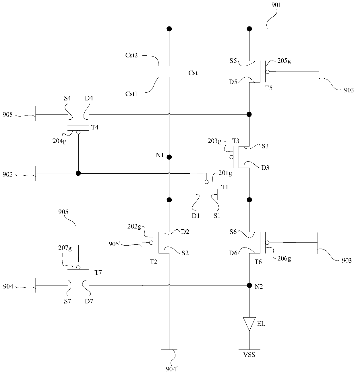
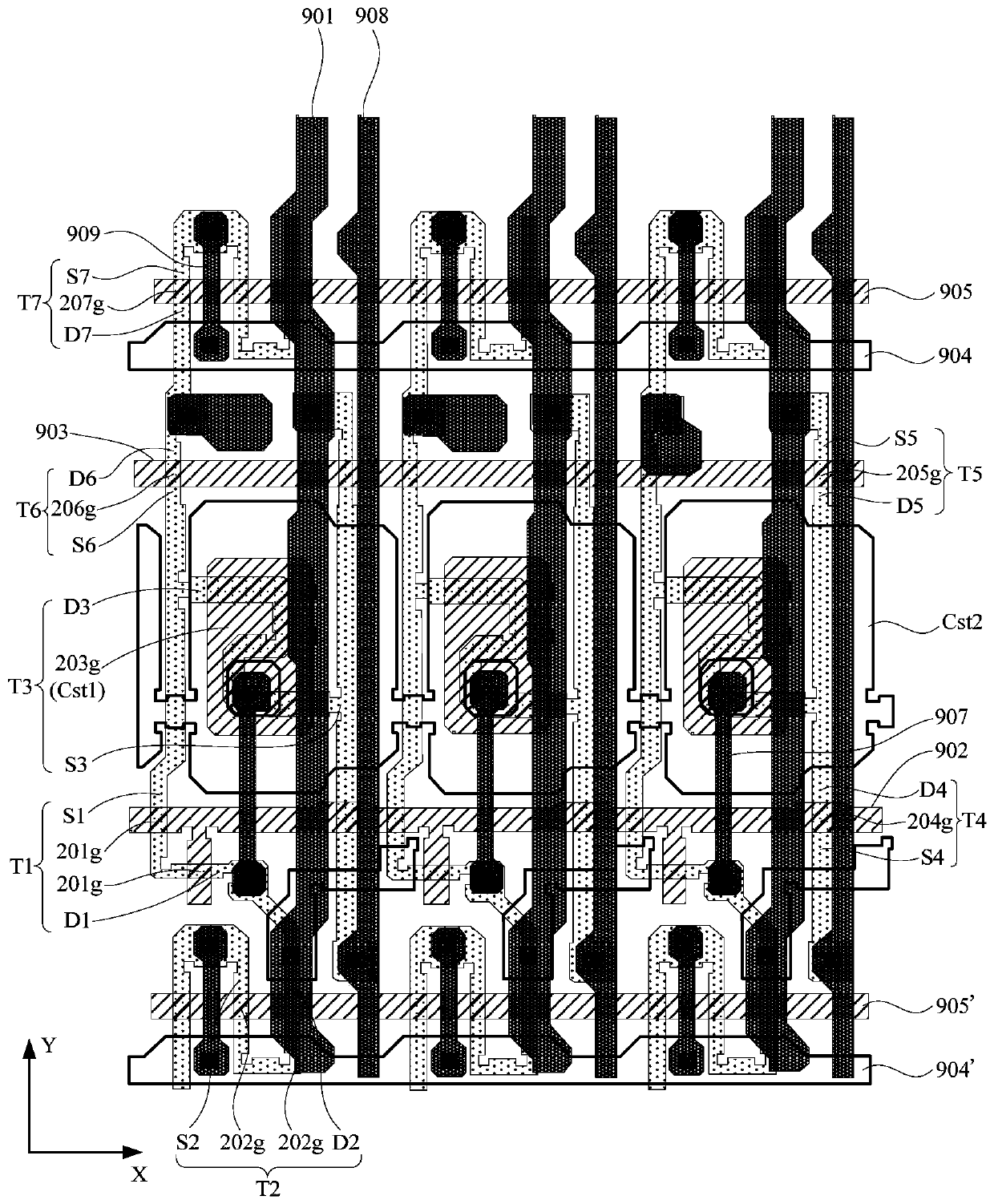
[0075] Such as image 3 and Figure 8 As shown, the present invention provides a display panel, which includes a plurality of pixel units distributed in an array, and each pixel unit includes a plurality of sub-pixels. Each sub-pixel includes a sub-pixel driving circuit, a power signal line pattern 901, a data line pattern 908, a gate line pattern 902, a light emission control signal line pattern 903, a reset signal line pattern 905, an initialization signal line pattern 904 and an anode pattern 320; At least part of the power signal line pattern 901 and the data line pattern 908 extend along the second direction; the gate line pattern 902, the light emission control signal line pattern 903, the reset signal line pattern...


PUM


Abstract

The invention provides a display panel, a manufacturing method thereof and a display device, relates to the technical field of the display, and aims to solve the problem that in the use process of a display product, water molecules in a flat layer escape and erode a light-emitting functional layer, so that the service life of the display product is shortened. The display panel comprises a substrate and a plurality of pixel units arranged on the substrate, the plurality of pixel units are distributed in an array, and each pixel unit comprises a plurality of sub-pixels; each sub-pixel comprisesa sub-pixel driving circuit, a flat layer and an anode pattern which are sequentially stacked; the anode patterns in at least part of the sub-pixels comprise middle parts and edge parts surrounding the middle parts; the surfaces, back to the substrate, of the flat layers are provided with grooves, the orthographic projections of the grooves on the substrate surrounds the orthographic projections of the middle parts on the substrate, and the orthographic projections of at least parts of the edge parts on the substrate are located in the orthographic projections of the grooves on the substrate.The display panel provided by the invention is used for displaying pictures.

Description

technical field [0001] The present invention relates to the field of display technology, in particular to a display panel, a manufacturing method thereof, and a display device. Background technique [0002] In an organic light-emitting diode (English: Organic Light-Emitting Diode; abbreviation: OLED) display product, the side of the anode layer facing away from the base of the display panel is provided with a light-emitting functional layer, and the side of the anode layer facing the base is provided with a flat layer. , the material of the flat layer is generally polyimide organic polymer, polyimide polymer material is generally formed by oligomer polymerization, the by-product of the polymerization reaction is water, and polyimide also has certain of water absorption. [0003] During the manufacturing process of the display panel, since the flat layer is covered by the anode layer with a dense structure, conventional heating methods cannot completely release the water mol...

Claims


Application Information

Patent Timeline
Patent Type & Authority Applications(China)
IPC IPC(8): H01L27/32H01L51/52H01L51/56G09G3/3225
CPCG09G3/3225H10K59/12H10K50/81H10K50/84H10K71/00H10K59/131H10K59/353H10K59/122H10K59/1213
Inventor 尚庭华周洋于鹏飞罗正位
Owner BOE TECH GRP CO LTD
Why Eureka
Try Eureka