Method of making starting material for chip fabrication comprising a buried silicon nitride layer

a technology of silicon nitride and starting material, which is applied in the direction of semiconductor devices, electrical apparatus, transistors, etc., can solve the problems of excessive nitrogen in the middle of the layer, undesirable bubbles, and nitrogen gas bubbles inside the layer

Inactive Publication Date: 2005-03-01
SILICON WAFER TECH
View PDF23 Cites 17 Cited by
  • Summary
  • Abstract
  • Description
  • Claims
  • Application Information

AI Technical Summary

Benefits of technology

[0029]It is an object of the present invention to provide a simple process for fabr...

Problems solved by technology

It further results in the capturing of excessive nitrogen in the middle of the layer and creating of nitrogen gas bubbles inside of the layer.
The bubbles are undesira...

Method used


Image

  • Method of making starting material for chip fabrication comprising a buried silicon nitride layer
  • Method of making starting material for chip fabrication comprising a buried silicon nitride layer
  • Method of making starting material for chip fabrication comprising a buried silicon nitride layer

Examples


Embodiment Construction

ic sectional views illustrating process flow steps for manufacturing a SOI substrate using separation by an implanted specie.

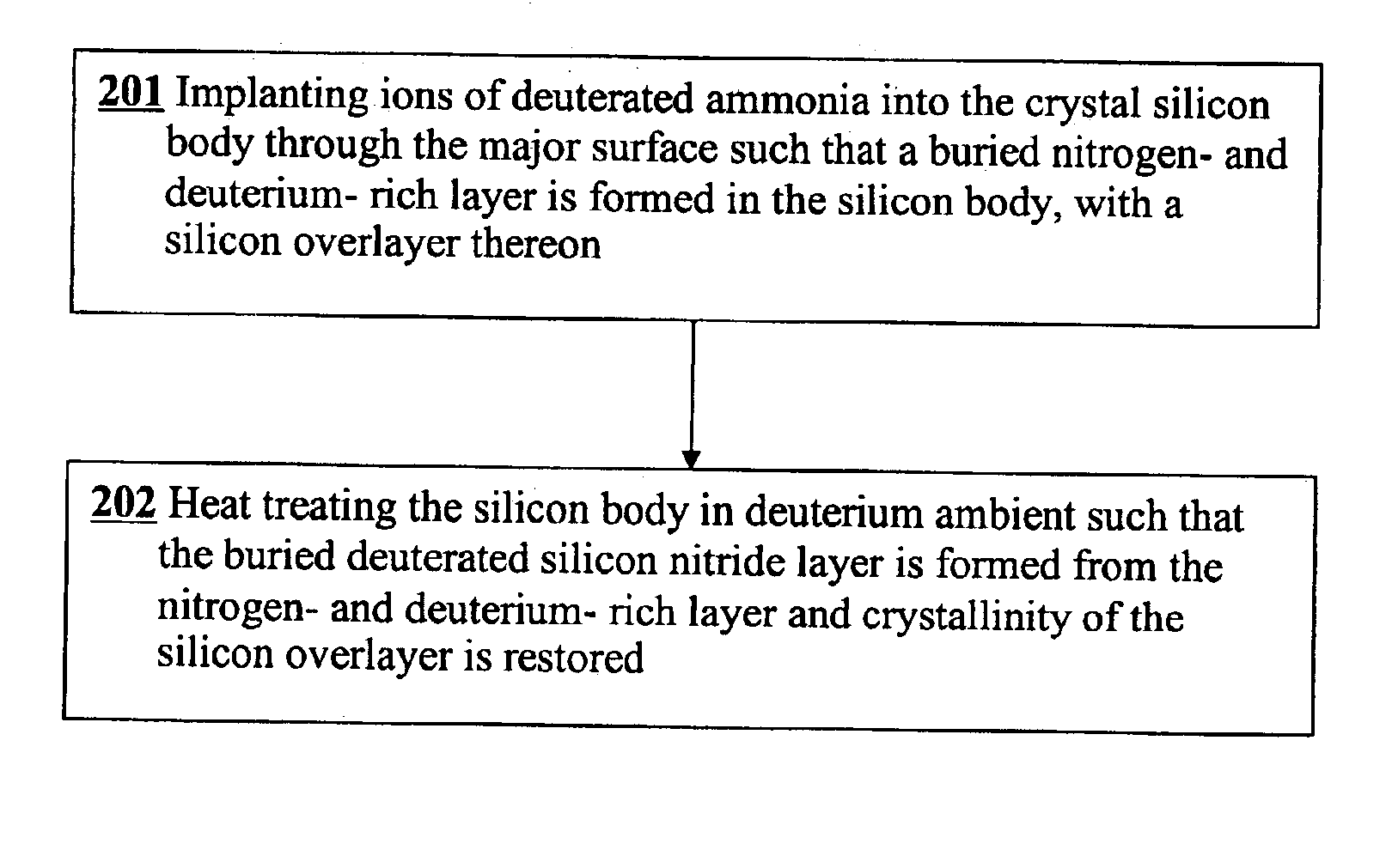
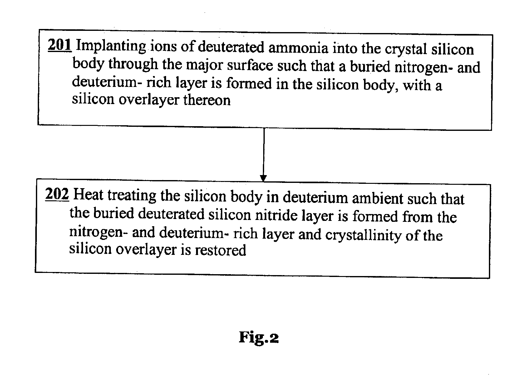
[0037]FIG. 2 shows the inventive process sequence due to the first preferred embodiment.

[0038]FIG. 3 shows the depth distribution of protium, deuterium, and nitrogen if they are implanted into a silicon wafer in form of ammonia (at 85 keV) or deuterated ammonia (at 100 keV).

[0039]FIG. 4 shows the depth distribution of protium, deuterium, and nitrogen if they are implanted into a silicon wafer in form of ammonia (at 850 keV) or deuterated ammonia (at 1 MeV).

[0040]FIG. 5 shows plots of projected ranges for nitrogen, deuterium, and protium as a function of implantation energy for implanted ND3 or NH3 ions.

[0041]FIG. 6 shows the inventive process sequence for to the second preferred embodiment

DETAILED DESCRIPTION OF THE FIRST PREFERRED EMBODIMENT

[0042]This invention allows one to fabricate SOI wafers with reduced thermal resistance between a single crystal silicon...


PUM


Abstract

The invention provides a method of making silicon-on-insulator SOI substrates with nitride buried insulator layer by implantation of molecular deuterated ammonia ions ND3+, instead of implanting nitrogen ions (N+, or N2+) as is done in prior art nitride SOI processes. The resultant structure, after annealing, has a buried insulator with a defect density which is substantially lower than in prior art nitride SOI. The deuterated nitride SOI substrates allow much better heat dissipation than SOI with a silicon dioxide buried insulator. These substrates can be used for manufacturing of high speed and high power dissipation monolithic integrated circuits.

Description

FIELD OF THE INVENTION[0002]The present invention relates generally to a fabrication method for silicon on-insulator (SOI) wafers. More particularly the present invention relates to a fabrication of the SOI with a deuterated silicon nitride insulative layer.BACKGROUND OF THE INVENTION[0003]Silicon-on-insulator (SOI) wafers are convenient starting material for semiconductor device (chip) fabrication. While the chips can be fabricated on bulk single crystal silicon, the use of the SOI gives advantages of better electrical insulation between individual devices (transistors), extended scaling down capabilities, and better performance of final chips. Two main process technologies for fabrication of SOI are known in prior art, (1) layer transfer, and (2) separation-by-implanted-specie.[0004]The layer transfer consists of the following process steps:[0005](1) a fragile plane inside of a donor wafer is created; the plane defines the boundary of a layer to be transferred;[0006](2) an insulat...

Claims


Application Information

Patent Timeline
IPC IPC(8): H01L21/70H01L21/762H01L29/786H01L29/66
CPCH01L29/78603H01L21/76243
Inventor USENKO, ALEXANDER
Owner SILICON WAFER TECH
Why Eureka
Try Eureka