Blooming control for a CMOS image sensor

a technology of cmos image sensor and bloom control, which is applied in the direction of pulse technique, radio frequency control device, instruments, etc., can solve the problems of displaying an affecting the brightness of certain areas of the output image, and most prevalent image defect in the output image. achieve the effect of high reset signal

Inactive Publication Date: 2005-03-01
OMNIVISION TECH INC
View PDF3 Cites 11 Cited by
  • Summary
  • Abstract
  • Description
  • Claims
  • Application Information

AI Technical Summary

Benefits of technology

The present invention is directed at a circuit for controlling the blooming effect in CMOS image sensors designed with a high voltage reset. In this regard, the circuit includes a high voltage supply circuit and a high voltage level shifter circuit. The high voltage supply circuit is configured to supply a voltage to the shifter circuit. The voltage has a voltage level higher than the absolute maximum voltage of the associated fabrication process. The shifter circuit is configured to output a high reset signal based on a reset signal generated to reset a pixel circuit of a pixel array. Instead of the reset signal, the high reset signal is coupled to a gate of the reset transistor in the pixel circuit. The high reset signal allows the reset transistor to maintain a gate to source potential less than the absolute maximum voltage associated with the fabrication process to avoid gate oxide breakdown even when the high reset signal is greater than the absolute maximum voltage. The high voltage level shifter circuit includes a high voltage inverter. The high voltage inverter is arranged to control the rising and falling edges of the RESETH signal. In addition, the high voltage inverter is arranged to raise the low level of the high reset signal by a predetermined voltage, thereby preventing a photodiode in the pixel circuit from becoming forward biased.

Problems solved by technology

Given certain conditions, digital pictures taken with a digital camera using complimentary metal-oxide semiconductor (CMOS) image sensors may display an image defect in the output image.
The image defect occurs most prevalently in output images with large contrasts.
The image defect makes certain areas within the output image appear brighter in comparison with the original image.
Thus, these additional charge carriers that are collected impact the read out of the output signal voltage for the neighboring pixel and will result in the image defect described above.
Firstly, the high voltage level shifter will dissipate significant power.
Therefore, blooming will occur in image sensors implementing a high voltage reset circuit.

Method used


Image

  • Blooming control for a CMOS image sensor
  • Blooming control for a CMOS image sensor
  • Blooming control for a CMOS image sensor

Examples


Embodiment Construction

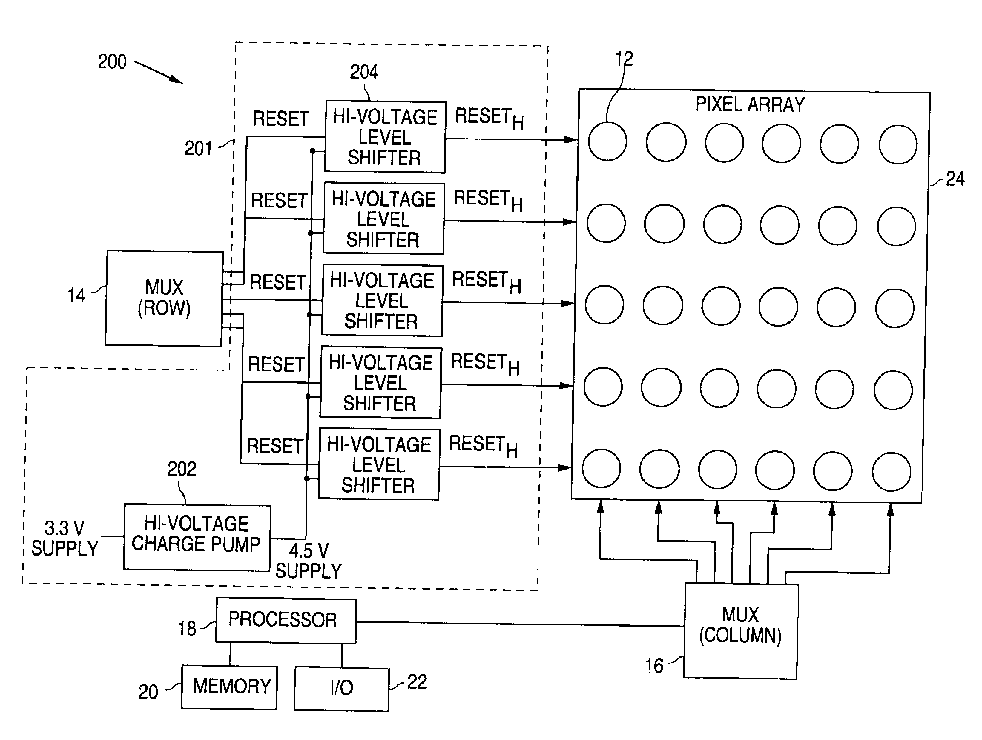
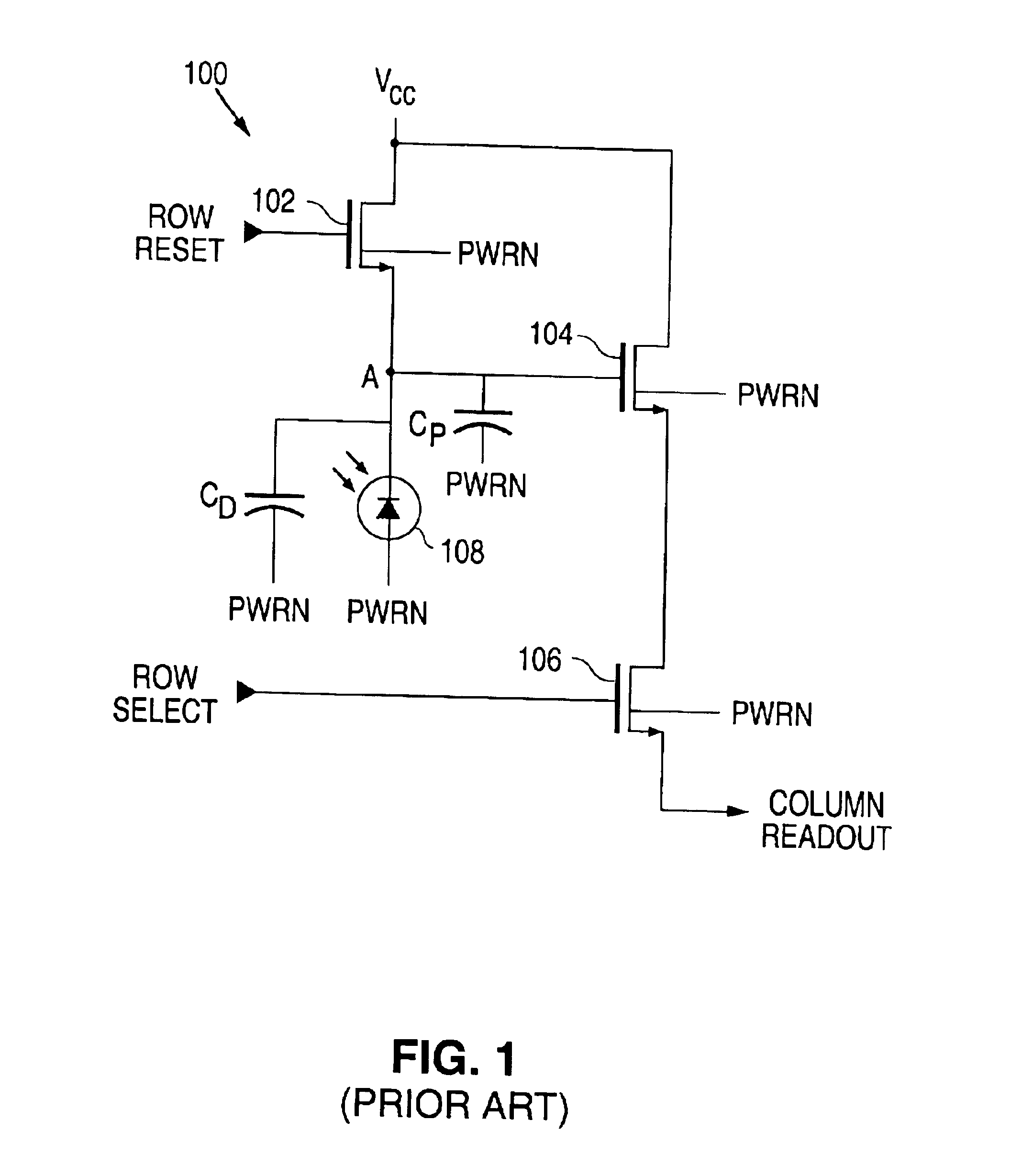
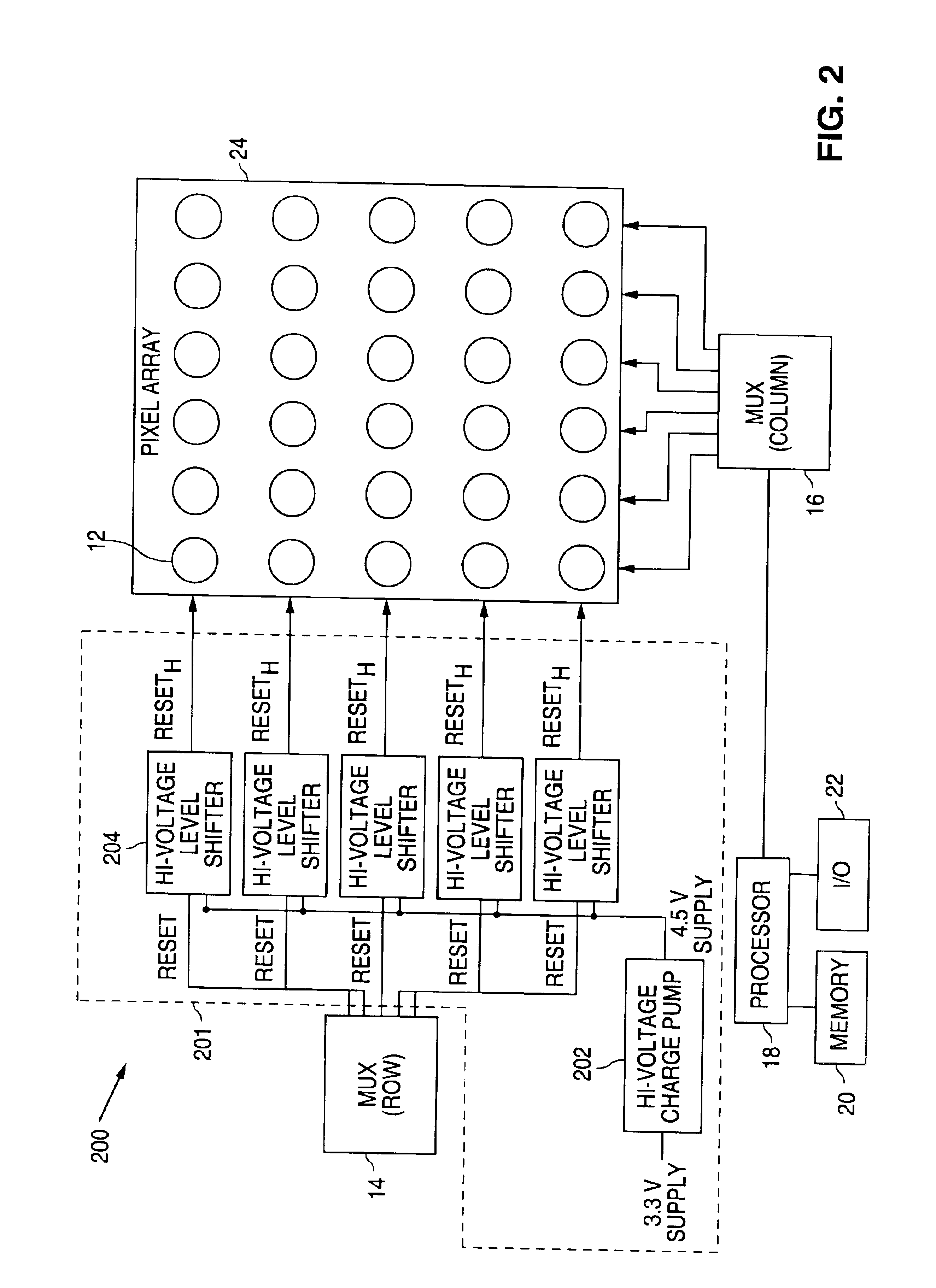
Briefly described, the present invention is directed at a circuit for controlling blooming within CMOS image sensors that are designed with a high voltage reset. FIG. 2 is a block diagram of an exemplary embodiment of several components for an image sensor employing a high voltage reset circuit. As shown, the image sensor 200 of the present invention includes an array 24 of individual pixel cells 12, such as pixel cell 100 shown in FIG. 1, arranged in columns and rows. A processor 18 is coupled to an input / output interface 22, a memory 20 and a row multiplexer 14, which is employed to reset and select each row of the pixel cell array 24. The processor 18 is also coupled to a column multiplexer 16 that is employed to read the value at each column for a selected row of pixel cells 12. The image sensor 200 further includes a high voltage reset circuit, shown generally within outlined box 201 and hereinafter referred to as high voltage reset circuit 201. The high voltage reset circuit 2...


PUM


Abstract

A high voltage reset circuit with blooming control that increases the dynamic range of a CMOS image sensor and prevents blooming from occurring in output images. The circuit includes a high voltage supply circuit and a high voltage level shifter circuit. The high voltage supply circuit is configured to supply a voltage to the shifter circuit. The voltage has a voltage level higher than the absolute maximum voltage of the associated fabrication process. The shifter circuit is configured to output a high reset signal based on a reset signal generated to reset a pixel circuit of a pixel array. Instead of the reset signal, the high reset signal is coupled to a gate of the reset transistor in the pixel circuit. The high reset signal allows the reset transistor to maintain a gate to source potential less than the absolute maximum voltage even when the high reset signal is greater than the absolute maximum voltage. The high voltage level shifter circuit includes a high voltage inverter arranged to raise the low level of the high reset signal by a predetermined voltage and to control the rising and falling edges of the RESETH signal. This prevents a photodiode in the pixel circuit from becoming forward biased and prevents blooming from occurring within the image sensor.

Description

FIELD OF THE INVENTIONThe present invention relates generally to CMOS image sensors, and more particularly to integrated CMOS transistor logic circuits for correcting a blooming effect within the CMOS image sensor.BACKGROUND OF THE INVENTIONGiven certain conditions, digital pictures taken with a digital camera using complimentary metal-oxide semiconductor (CMOS) image sensors may display an image defect in the output image. The image defect occurs most prevalently in output images with large contrasts. The image defect makes certain areas within the output image appear brighter in comparison with the original image. For example, if the original image has a very bright spot surrounded by a dark area, the output image will display the dark area as being brighter than the dark area in the original image.This image defect is caused by a phenomenon commonly referred to as “blooming.” Blooming occurs when neighboring pixels collect electrons that have been injected into the substrate by a...

Claims


Application Information

Patent Timeline
Patent Type & Authority Patents(United States)
IPC IPC(8): H01L27/00H01L27/146
CPCH01L27/14654
Inventor PHAN, CHRISTINA P.
Owner OMNIVISION TECH INC
Why Eureka
Try Eureka