Check patentability & draft patents in minutes with Patsnap Eureka AI!

High-speed programmable read-only memory (PROM) devices

a programmable read-only memory and high-speed technology, applied in solid-state devices, instruments, basic electric elements, etc., can solve the problems of misreading rom data, rom has a longer time interval, and rom is longer, so as to improve operation speed and memory cell structure, the effect of high speed

Inactive Publication Date: 2005-03-01
SAMSUNG ELECTRONICS CO LTD
View PDF4 Cites 16 Cited by
  • Summary
  • Abstract
  • Description
  • Claims
  • Application Information

AI Technical Summary

Benefits of technology

To solve the above problems, it is a first objective of the present invention to provide a high speed programmable ROM system which improves a operation speed, and a memory cell structure therefor.

Problems solved by technology

However, the embedded diffusion-programmable ROM has a longer time interval from when data from a user is received to when a completed product is manufactured, that is, the turn-around time of the embedded diffusion-programmable ROM is longer than that of the embedded metal-programmable ROM.
If this ratio is big, the transition in the neighboring line interferes the bit line, and the bit line which is precharged may not be able to maintain the precharged state and therefore may cause to misread ROM data.
For this, the total capacitance loaded on a bit line should be increased, but this causes a decrease in speed.

Method used


Image

  • High-speed programmable read-only memory (PROM) devices
  • High-speed programmable read-only memory (PROM) devices
  • High-speed programmable read-only memory (PROM) devices

Examples


Embodiment Construction

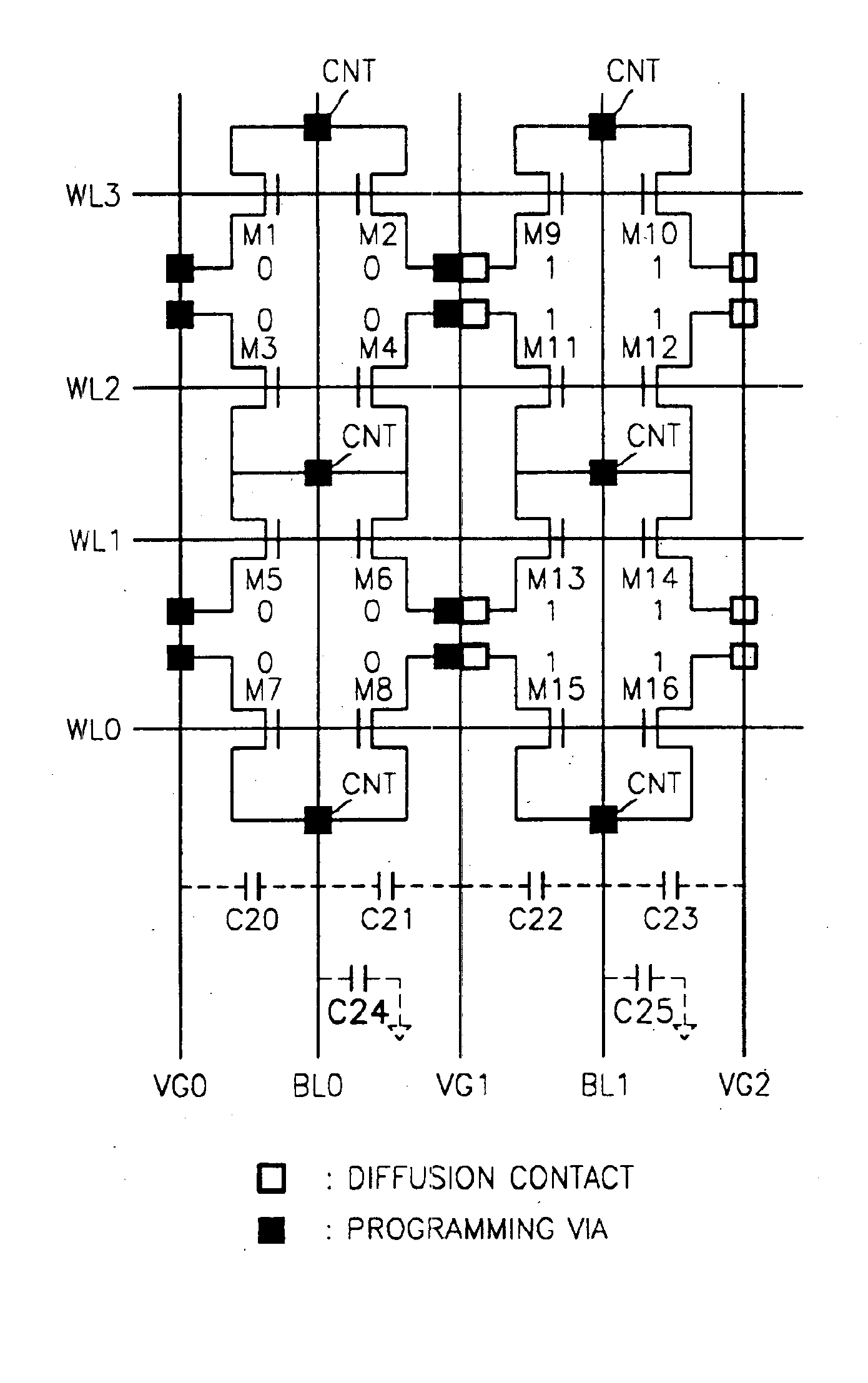
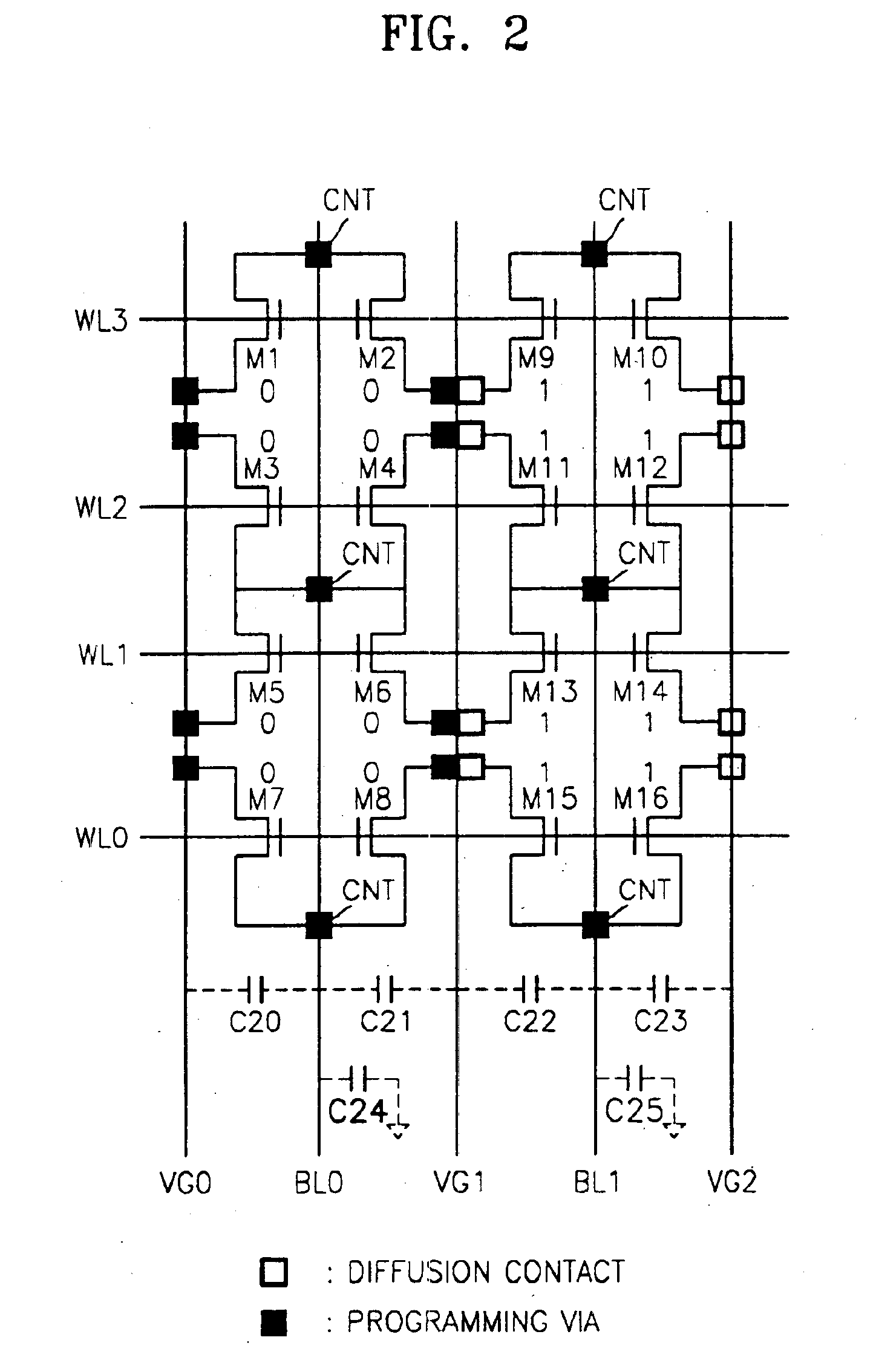
FIG. 2 is a circuit diagram showing a preferred embodiment of the cell array structure of a high speed programmable ROM according to the present invention.

For convenience of explanation, FIG. 2 shows a 4×4 bit cell array structure formed with 2 bit lines BL0 and BL1, 3 virtual ground lines VG0˜VG2, 4 word lines WL0˜WO3, and 16 NMOS transistors M1˜M16. Here, capacitors C20˜C23 of FIG. 1 show not actual circuit elements but coupling capacitance between lines. C24 is a total capacitance loaded on bit line BL0, and C25 is a total capacitance loaded on bit line BL1. Also for convenience of explanation, the programmable ROM shown in FIG. 2 is assumed to be a via programmable ROM of which ROM data programming is performed in a via processing process.

Referring to FIG. 2, the drain of each of cell transistors M1˜M8 is connected to bit line BL0, and the drain of each of cell transistors M9˜M10 is connected to bit line BL1. At this time, in the structure shown in FIG. 2, four cell transistors ...


PUM


Abstract

A high speed programmable ROM, a memory cell structure therefor, and a method for writing data on / reading data from the programmable ROM are provided. The programmable ROM system has a plurality of memory cell, each of which has a gate, a first electrode, and a second electrode; a plurality of word lines, each of which is connected to the gates of a predetermined number of cells of the plurality of memory cells; a plurality of bit lines, each of which is connected to the first electrodes of a predetermined number of memory cells of the plurality of memory cells and is arranged in a direction substantially perpendicular to the word lines; and a plurality of virtual ground lines, each of which is selectively connected to ground in response to control signals, and is arranged in a direction actually perpendicular to the word lines, wherein the plurality of memory cells are programmed to predetermined logic levels by selectively connecting the second electrode of each of the plurality of memory cells to the plurality of virtual ground lines. The high speed programmable ROM system selectively connects the source of a cell transistor to a virtual ground line according to ROM data such that the capacitance of a bit line can be maintained at a predetermined level without becoming excessively great or small. Thus, the operation speed of the programmable ROM increases and misreading programmed data is minimized.

Description

BACKGROUND OF THE INVENTION1. Field of the InventionThe present invention relates to a semiconductor memory device, and more particularly, to a high speed programmable Read Only Memory (ROM) system.2. Description of the Related ArtMask ROM is a semiconductor memory device in which a user codes needed data in advance on the memory device in a manufacturing process so that the coded data can be repeatedly read later. Mask ROMs include an embedded diffusion-programmable ROM and an embedded metal-programmable ROM. For the embedded diffusion-programmable ROM, a ROM data code is determined in a diffusion process in the manufacturing processes, while for the embedded metal-programmable ROM, a ROM data code is determined in a metal processing process in the manufacturing processes.Meanwhile, there is an embedded contact programmable ROM or an embedded via programmable ROM which is almost the same as the embedded metal-programmable ROM. For the embedded contact programmable ROM, a ROM data c...

Claims


Application Information

Patent Timeline
IPC IPC(8): G11C17/12G11C17/08G11C17/18
CPCG11C17/126
Inventor LEE, JOONG-EONLEE, YOUNG-KEUNCHOO, YONG-JAEDO, YOUNG-SOOK
Owner SAMSUNG ELECTRONICS CO LTD
Features
  • R&D
  • Intellectual Property
  • Life Sciences
  • Materials
  • Tech Scout
  • Unparalleled Data Quality
  • Higher Quality Content
  • 60% Fewer Hallucinations
Learn More