Wafer level chip size package having rerouting layers

a technology of rerouting layer and wafer level, which is applied in the direction of semiconductor/solid-state device testing/measurement, semiconductor device details, semiconductor/solid-state device testing/measurement, etc., can solve the problems of long turn around time from an order to a delivery, unnecessary stock holding, and inability to change the operation mode after a chip, etc., to reduce the stock held by anticipated production, shorten the turn around time of a wafer level csp, and reduce the stock holding

Inactive Publication Date: 2005-03-01
RENESAS ELECTRONICS CORP
View PDF9 Cites 66 Cited by
  • Summary
  • Abstract
  • Description
  • Claims
  • Application Information

AI Technical Summary

Benefits of technology

It is an object of the present invention to provide a technique that shortens a turn around time of a wafer level CSP.
It is another object of the present invention to provide a technique that reduces the manufacturing cost of a wafer level CSP.
It i

Problems solved by technology

On the other hand, since a wafer level CSP starts a wafer process after a product type has been fixed and performs steps until formation of external connection terminals (solder bumps) in the wafer process, operation modes cannot be changed after a chip is divided into chips.
Therefore, a turn around time from an order to a

Method used


Image

  • Wafer level chip size package having rerouting layers
  • Wafer level chip size package having rerouting layers
  • Wafer level chip size package having rerouting layers

Examples


embodiment 2

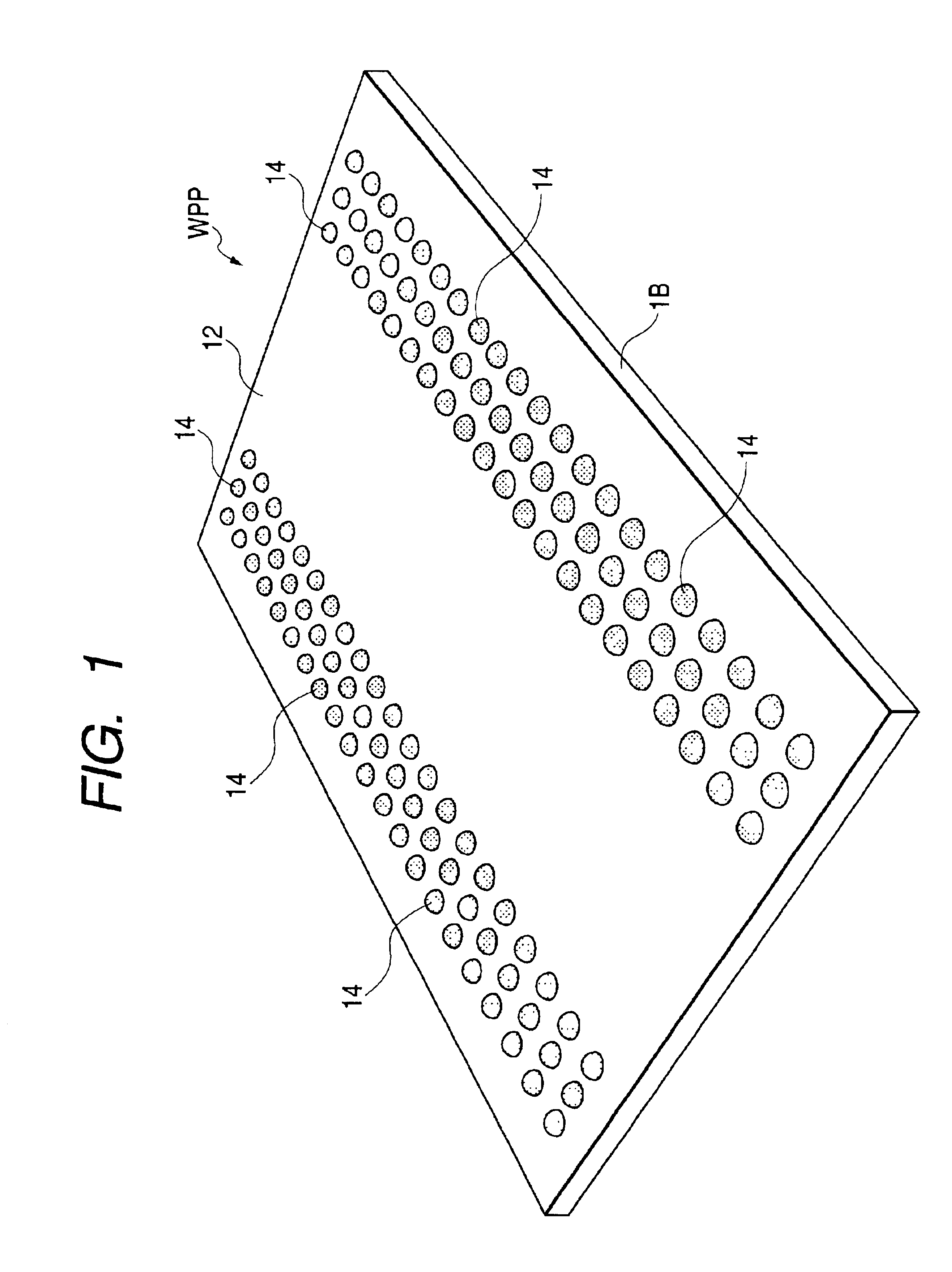
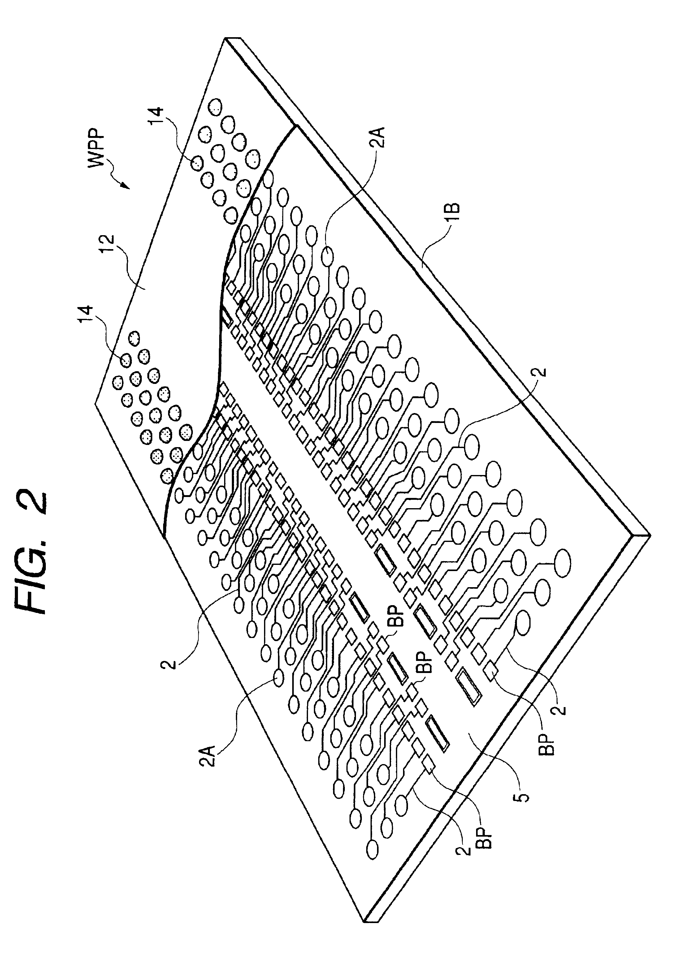
FIG. 26 is a flow chart of the steps in manufacturing a semiconductor integrated circuit device, i.e., a WL-CSP according to Embodiment 2, FIG. 27 is a sectional view of a main part of a wafer in a semiconductor wafer holding state shown in the manufacturing flow chart in FIG. 26. FIGS. 28 to 34 are sectional views showing main parts of the steps of an organic passivation layer after a product type is fixed to the step of forming bumps.

In Embodiment 2, as is apparent from the manufacturing flow chart in FIG. 26, a semiconductor wafer 1 to which a wafer test and a probe test are performed is stocked, product types are fixed, and a rerouting pattern is selectively formed for each product type. Thereafter, the semiconductor wafer 1 is cut into a plurality of semiconductor chips, and the semiconductor chips are separated from each other, so that WL-CSPs are formed. The steps performed until the wafer is stocked are substantially the same as those in Embodiment 1. FIG. 27 is a sectional ...

embodiment 3

FIGS. 35, 36, and 37 are manufacturing flow charts showing methods of manufacturing semiconductor integrated circuit devices according to Embodiment 3, i.e., WL-CSPs. In each of the manufacturing methods shown in FIGS. 36, 37, and 38, as in Embodiments 1 and 2, a semiconductor wafer is stocked in advance, a product type is fixed, and rerouting layers depending on the product type are formed. Unlike Embodiments 1 and 2, an organic passivation layer is formed before the semiconductor wafer is stocked.

When the organic passivation layer is formed in advance as described above, damage to a semiconductor wafer when the semiconductor wafer is conveyed and stocked can be reduced.

The manufacturing method shown in FIG. 36 is a method in which rerouting layers are formed on the organic passivation layer after a product type is fixed. The steps performed until a product is completed after a product type is fixed can be more reduced in number.

In the manufacturing method shown in FIG. 37, an elas...

embodiment 4

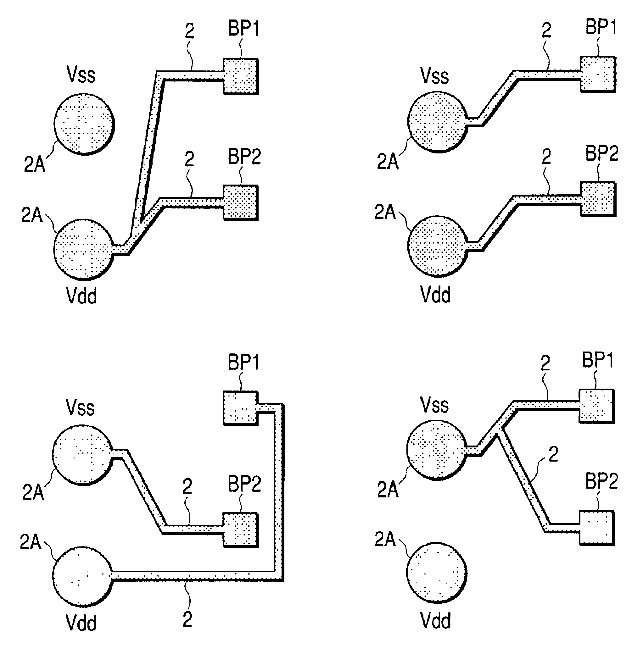
FIG. 38 is a sectional view of a semiconductor integrated circuit device, i.e., a WL-CSP according to Embodiment 4. In the WL-CSP shown in FIG. 38, bonding pads 42 formed on a peripheral portion of one major surface of a semiconductor chip 41 are connected to solder bumps 47 with rerouting layers 44. The rerouting layers 44 are formed of copper, and are constituted by wiring portions 44A and 44B and a copper post (columnar part) 44C. Such a structure is also stocked in a wafer state, rerouting layers having different patterns are formed depending on product types after the product types are fixed, so that a plurality of WL-CSPs of different types can be manufactured from the wafer on which LSIs of one type are formed.


PUM


Abstract

A semiconductor integrated circuit device includes a semiconductor substrate, a circuit element formed on one major surface of the semiconductor substrate and constituting an integrated circuit having a plurality of functions or a plurality of characteristics, an internal connection terminal, connected to the integrated circuit, for selecting one of the plurality of functions or one of the characteristics in the integrated circuit, an insulating layer covering the internal connection terminal such that the internal connection terminal is selectively exposed, and an external connection terminal arranged on the insulating layer. One of the plurality of functions or one of the plurality of characteristics is selected by a connection state between the internal connection terminal and the external connection terminal.

Description

TECHNICAL FIELD OF THE INVENTIONThe present invention relates to a semiconductor integrated circuit device and a method of manufacturing the same, and a technique which is effectively applied to a CSP (chip size package), i.e., a so-called wafer level CSP (WL-CSP) or a wafer process package which is a scheme in which a packaging step is completed in a wafer state.BACKGROUND OF THE INVENTIONA scheme in which a packaging process (post-process) and a wafer process (pre-process) are integrated to each other to complete a packaging step in a wafer state, i.e., a technique so-called a wafer level CSP has the following advantage. That is, since a packaging process is performed by applying a wafer process, the number of steps can be made considerably smaller than that of a conventional method in which a packaging process (post-process) is performed to each chip cut from a wafer. The wafer level CSP is also called a wafer process package (WPP).In the wafer level CSP, a wiring layer in the CS...

Claims


Application Information

Patent Timeline
IPC IPC(8): H01L23/52H01L23/31H01L23/28H01L21/66H01L23/538H01L21/3205H01L21/312H01L21/822H01L23/12H01L23/48H01L27/04
CPCH01L22/22H01L23/3114H01L24/13H01L23/5382H01L2924/13091H01L2924/1306H01L2224/11H01L2924/10253H01L2223/54406H01L2924/12044H01L2924/19041H01L2924/3011H01L2924/00H01L24/02H01L24/03H01L24/05H01L2224/02379H01L2224/05001H01L2224/05008H01L2224/05024H01L2224/05548H01L2224/05571H01L2224/0615H01L2924/0001H01L2924/12042H01L2924/14H01L2924/351H01L2224/05644H01L2924/00014H01L2224/05147H01L2224/05171H01L2224/02H01L23/48
Inventor MIYAMOTO, TOSHIOANJO, ICHIRONISHIMURA, ASAOKATAGIRI, MITSUAKISHIRAI, YUJIYAMAGUCHI, YOSHIHIDE
Owner RENESAS ELECTRONICS CORP
Why Eureka
Try Eureka