Phase controlled oscillator circuit with input signal coupler

a phase control and oscillator circuit technology, applied in the direction of oscillator generators, pulse generation by logic circuits, pulse techniques, etc., can solve the problem of increased jitter of the clock multiplier

Inactive Publication Date: 2005-03-01
RAMBUS INC
View PDF5 Cites 79 Cited by
  • Summary
  • Abstract
  • Description
  • Claims
  • Application Information

AI Technical Summary

Benefits of technology

In certain embodiments, the frequency of the input signal is about equal to the resonant frequency. The oscillator may amplify the input signal. The oscillator may filter the input signal such as to filter pulse width variations of the input signal. When comb

Problems solved by technology

PLL clock multipliers suffer from increased jitter because they integrate phase error over many

Method used


Image

  • Phase controlled oscillator circuit with input signal coupler
  • Phase controlled oscillator circuit with input signal coupler
  • Phase controlled oscillator circuit with input signal coupler

Examples


Embodiment Construction

A description of preferred embodiments of the invention follows.

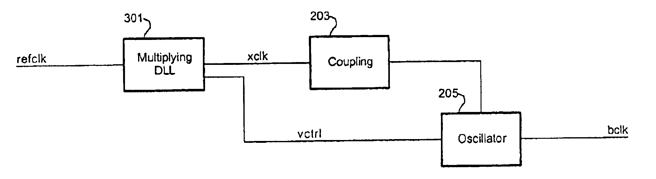
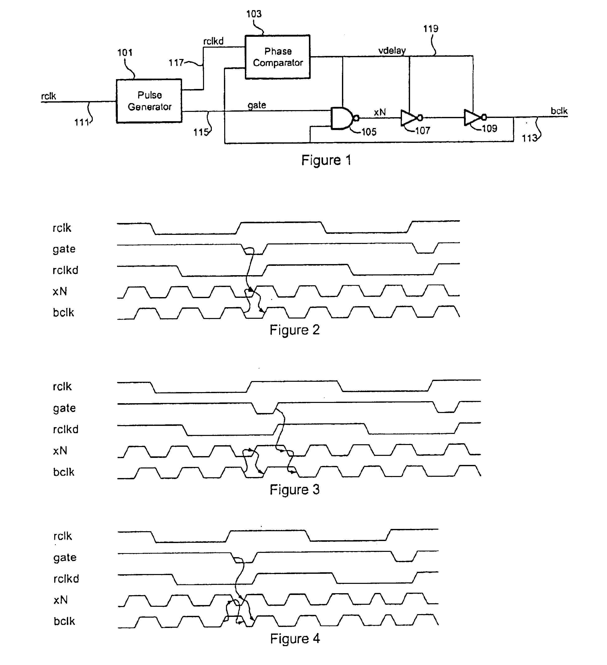
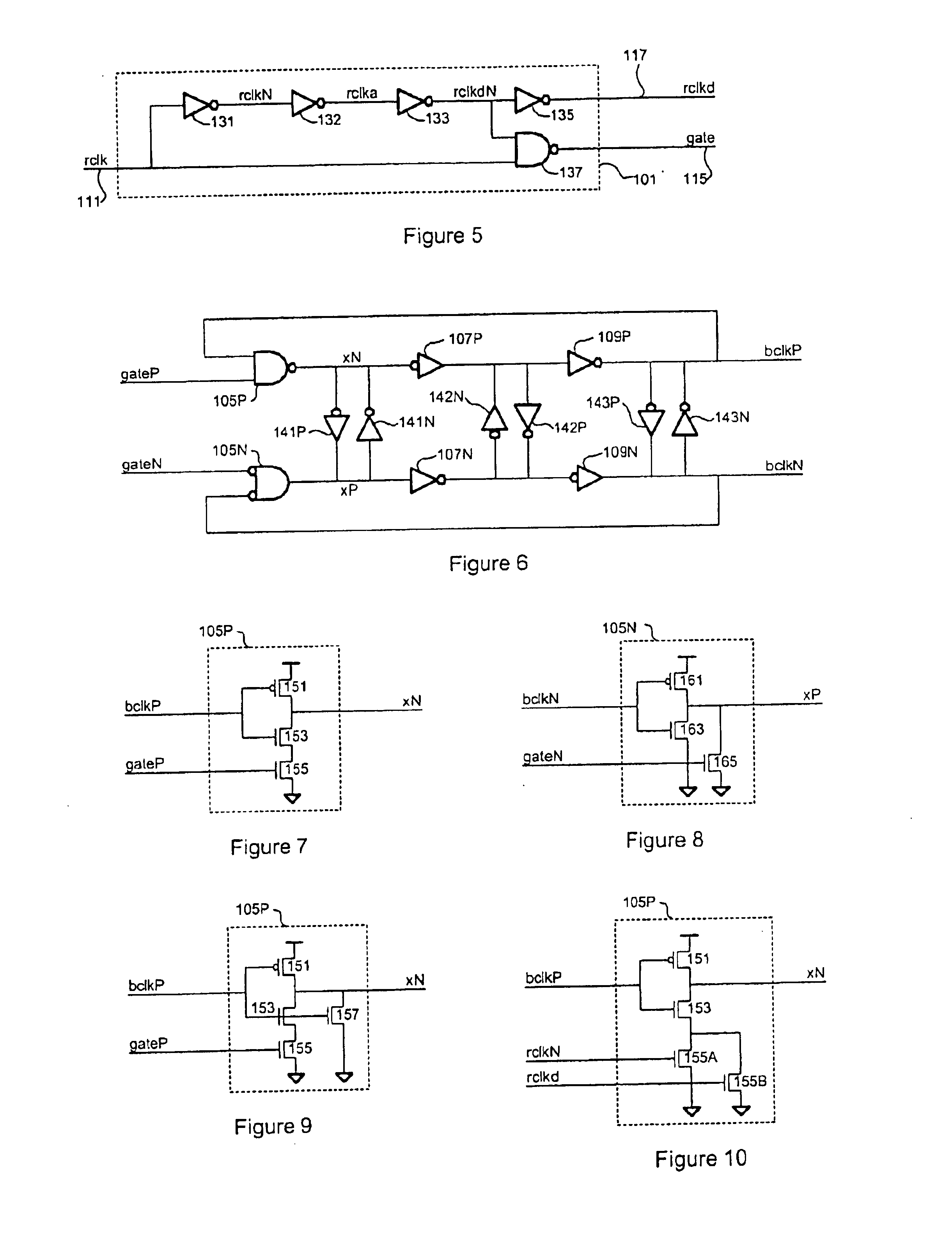
FIG. 1 shows a clock multiplier realized using a stoppable oscillator. NAND-gate 105, and inverters 107 and 109 form a voltage-controlled ring oscillator. This oscillator free-runs, generating bclk, as long as the gate signal is high. When the gate signal is low, the oscillator is stopped with the bclk output low. The oscillator frequency is set via a control voltage, Vdelay, that is adjusted by comparing the phase of bclk to the phase of a delayed referenced clock, rclkd, in phase comparator 103. In the preferred embodiment, phase comparator 103 is realized as a combined phase comparator and charge pump as described in pending patent application Ser. No. 09 / 414,761, filed Oct. 7, 1999, the entire teachings of which are incorporated herein by reference.

A combined phase comparator and charge pump circuit is illustrated in FIG. 42. This circuit accepts both polarities of two clocks, bclk and fclk, and a window signal that...


PUM


Abstract

An oscillating signal in an oscillator is caused to phase shift toward the phase of an input signal coupled to the oscillating signal. The resonant frequency of the oscillator is about equal to an integer multiple of the frequency of the input signal. The input signal may be generated in a pulse generator to have an input pulse duration less than or equal to that of the oscillating signal. The oscillator circuit may be used as a filter to filter pulse width variations or to filter jitter from a reference clock. The oscillator circuit may also serve as a buffer by amplifying the input signal. Phase interpolation can be obtained by coupling at least one input signal with at least one oscillating signal.

Description

BACKGROUND OF THE INVENTIONCommunication circuits use clock multipliers to convert a lower frequency reference clock, rclk, to a higher frequency bit clock, bclk. For example, the preferred embodiment uses a clock multiplier to convert a 156 MHz reference clock to a 1.248 GHz bit clock, a multiplication factor of eight. As described in pending patent application Ser. No. 09 / 557,640, filed Apr. 25, 2000, prior art communication systems have employed phase-locked loops (PLLs) and delay-locked loops (DLLs) to perform clock multiplication. PLL clock multipliers suffer from increased jitter because they integrate phase error over many reference clock cycles, and DLL-based clock multipliers introduce jitter due to device mismatch. The above referenced application shows how a multiplying-DLL-based clock multiplier can be used to give low jitter by eliminating both of these effects.SUMMARY OF THE INVENTIONThe present invention relates to improvements in an oscillator circuit by which its ph...

Claims


Application Information

Patent Timeline
IPC IPC(8): H03L7/081H03K3/00H03L7/099H03K3/03H03L7/091H03L7/08H03L7/20H03L7/083H03L7/24H03L7/16H03K3/354H03L7/00H03L7/23
CPCH03K3/0315H03K3/0322H03K3/354H03L7/07H03L7/0805H03L7/0812H03L7/0998H03L7/091H03L7/0995H03L7/20H03L7/23H03L7/24H03L7/083H03L7/0816H03L7/0818
Inventor DALLY, WILLIAM J.FARJAD-RAD, RAMINPOULTON, JOHN W.GREER, III, THOMAS H.NG, HIOK-TIAQSTONE, TEVA J.
Owner RAMBUS INC
Why Eureka
Try Eureka