

Defect detection system
a detection system and defect technology, applied in the field of defect detection, can solve the problems of inability to provide information useful for detecting defects on the wafer, single detector output becomes saturated, and system optimization is typically not optimized for such purposes, so as to facilitate the process of real-time defect classification and reduce cross-talk
- Summary
- Abstract
- Description
- Claims
- Application Information
AI Technical Summary
Benefits of technology
Problems solved by technology
Method used
Image

Examples
Embodiment Construction
4]FIGS. 9B and 9C are schematic views of filter wheels useful in the embodiment of FIG. 9A.
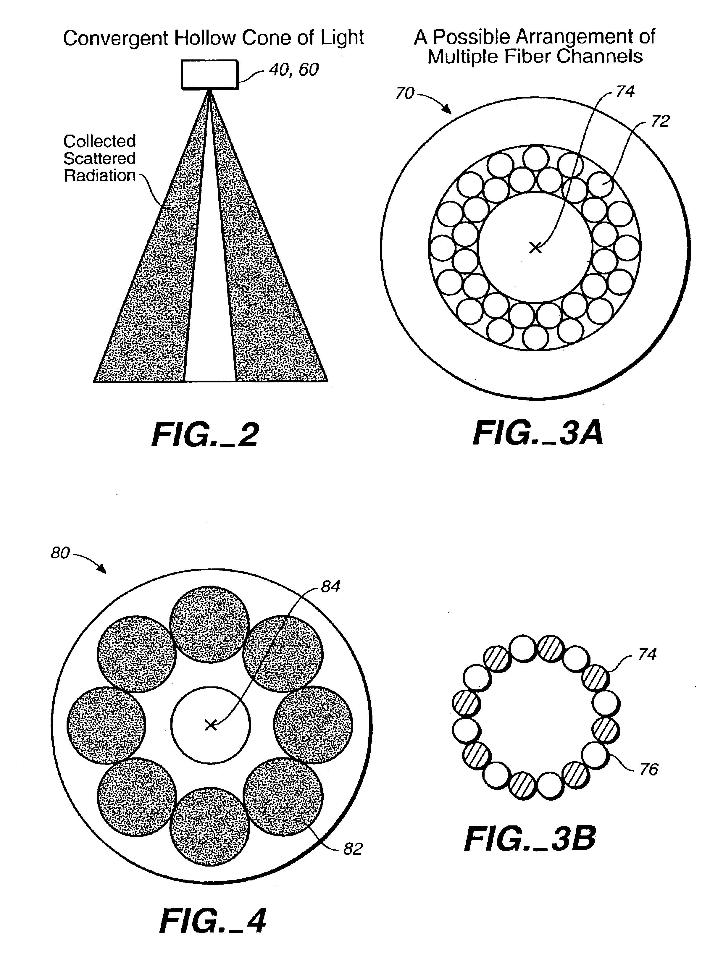
[0035]FIG. 10 is a schematic view of a two-dimensional diffraction components from a pattern on a surface to be inspected illustrating an aspect of the invention.
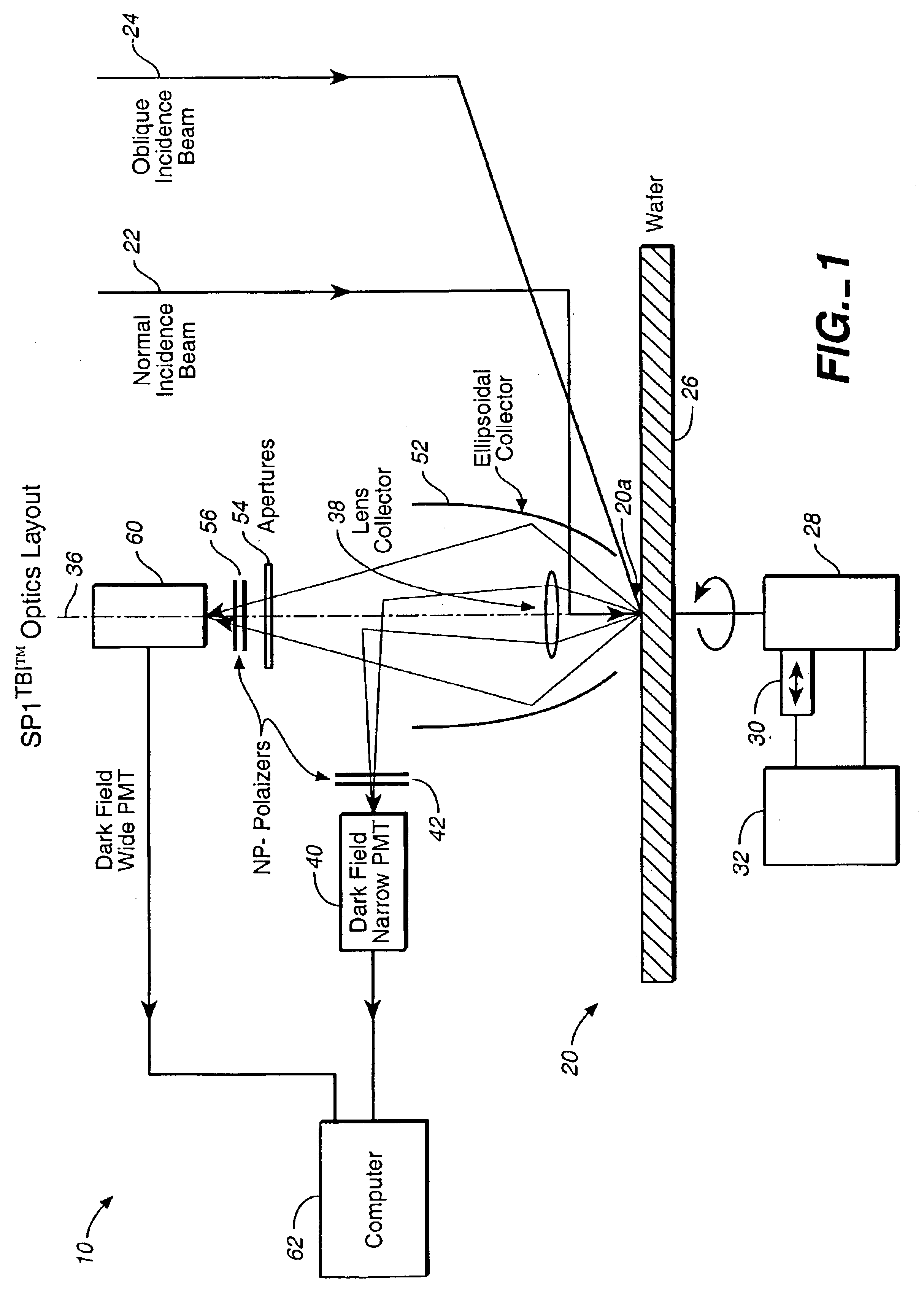
[0036]FIG. 11 is a schematic view of a defect inspection system to illustrate one more alternative embodiment of the invention.
[0037]FIG. 12 is a schematic view of an asymmetric mask for use in the different embodiments of this invention.
[0038]FIGS. 13A and 13B are schematic views of two masks used with the different systems of this application to illustrate yet another aspect of the invention.
[0039]FIG. 14 is a graphical plot of the interference intensity of thin film surfaces when illuminated with radiation of three different polarizations to illustrate another aspect of the invention.
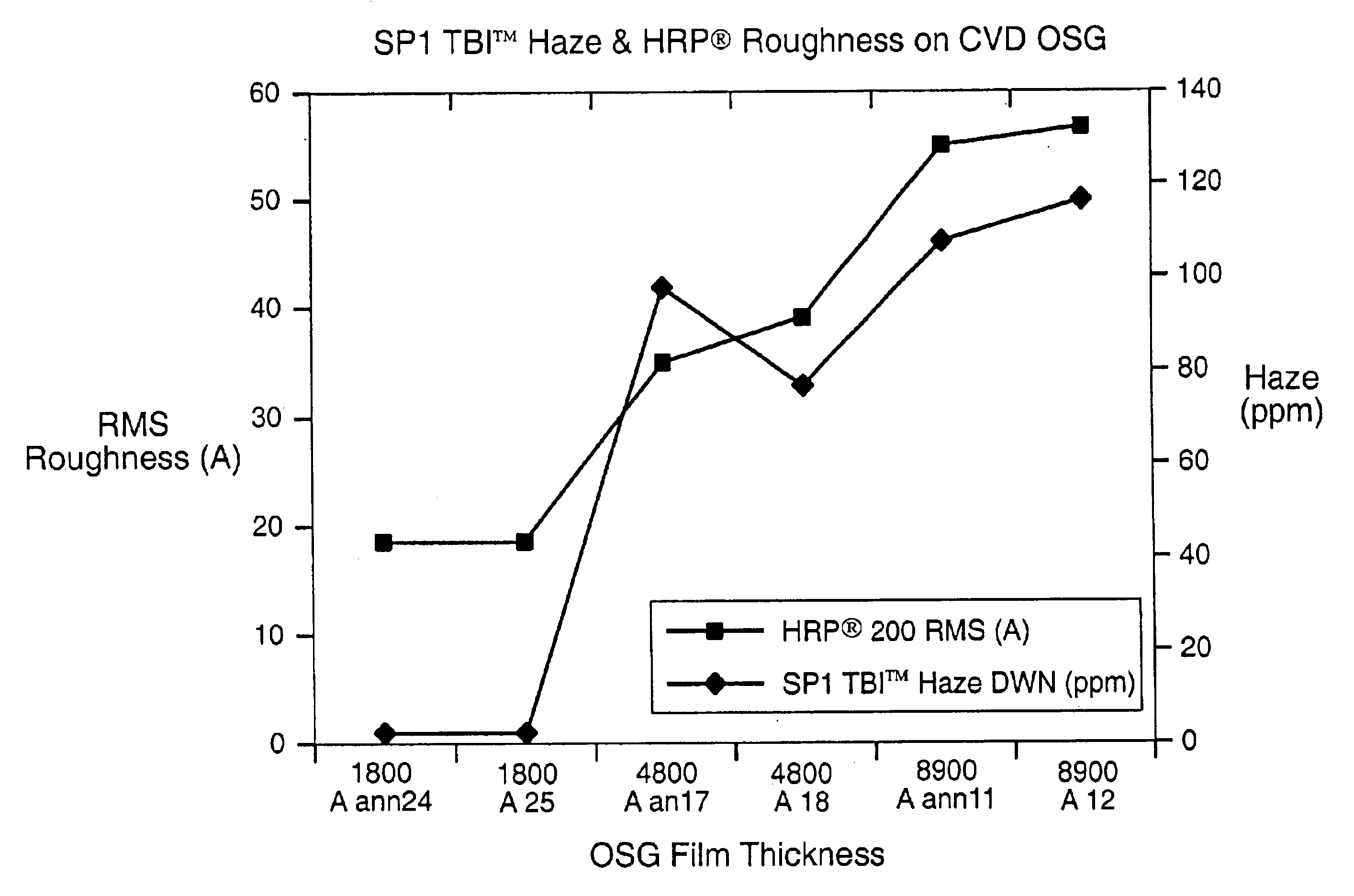
[0040]FIG. 15 is a graphical plot of haze and surface roughness to illustrate yet another aspect of the invention.
[0041]FIG. 16 is a block diagram ill...
PUM
| Property | Measurement | Unit |
|---|---|---|
| elevational collection angles | aaaaa | aaaaa |
| cell size | aaaaa | aaaaa |
| cell size | aaaaa | aaaaa |
Abstract
Description
Claims
Application Information