Via density rules

a density rule and density rule technology, applied in the field of semiconductor device manufacturing, can solve problems such as resistance shift failures

Active Publication Date: 2005-03-08
INFINEON TECH AG
View PDF6 Cites 14 Cited by
  • Summary
  • Abstract
  • Description
  • Claims
  • Application Information

AI Technical Summary

Problems solved by technology

In interconnect structures, the connecting vias between metal layers are subject to significant the...

Method used


Image

  • Via density rules
  • Via density rules
  • Via density rules

Examples


Embodiment Construction

While the making and using of various embodiments of the present invention are discussed herein in terms of specific geometries, it should be appreciated that the present invention provides many inventive concepts that can be embodied in a wide variety of contexts. The specific embodiments discussed herein are merely illustrative of specific ways to make and use the invention, and are not meant to limit the scope of the invention.

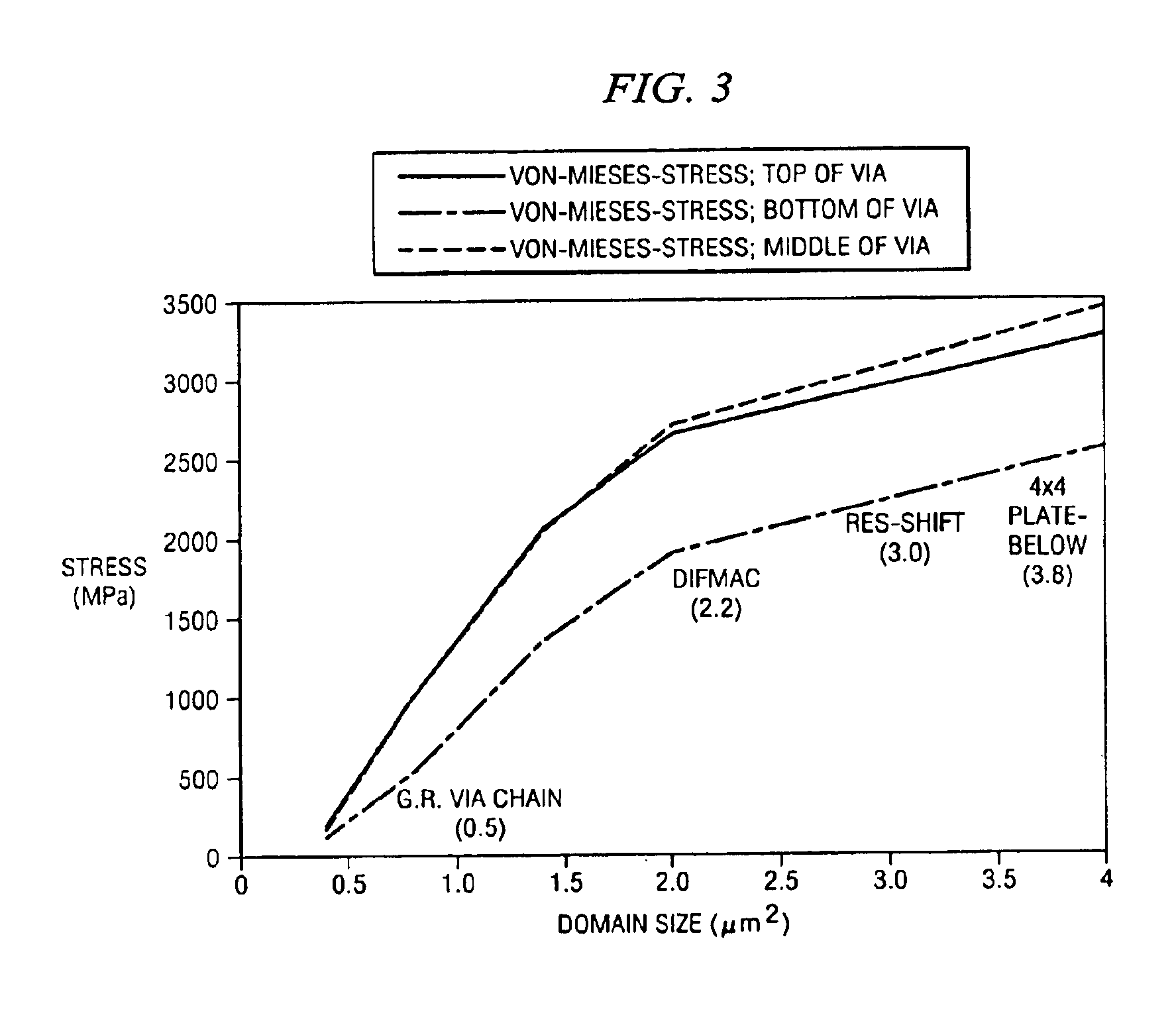
The present invention can reduce the thermo-mechanical stress on vias and thereby reduce related failures. Exemplary embodiments of the present invention can provide a via-to-metal area ratio at least as large as a predetermined value below which the additional stress on the vias does not significantly increase.

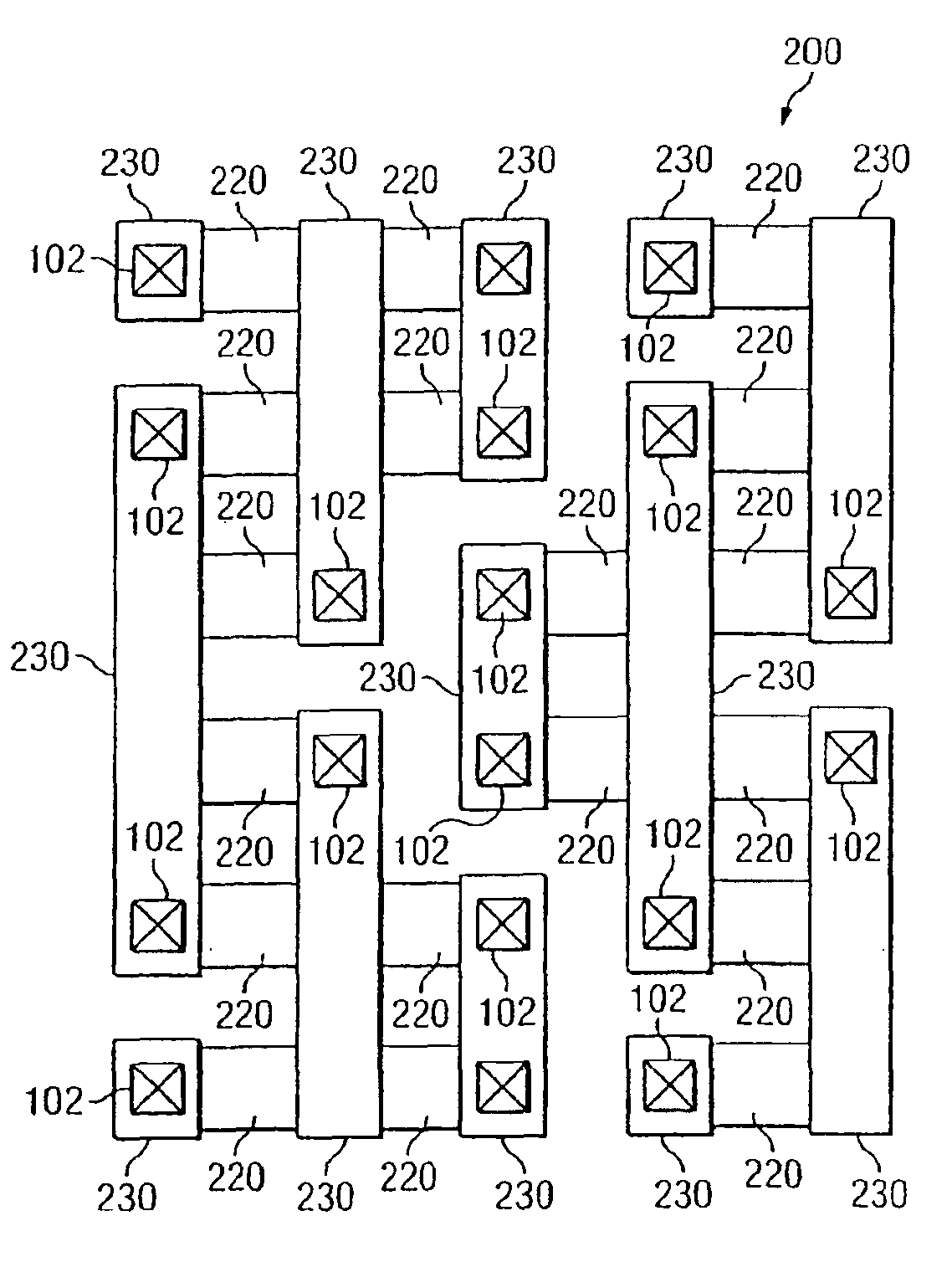
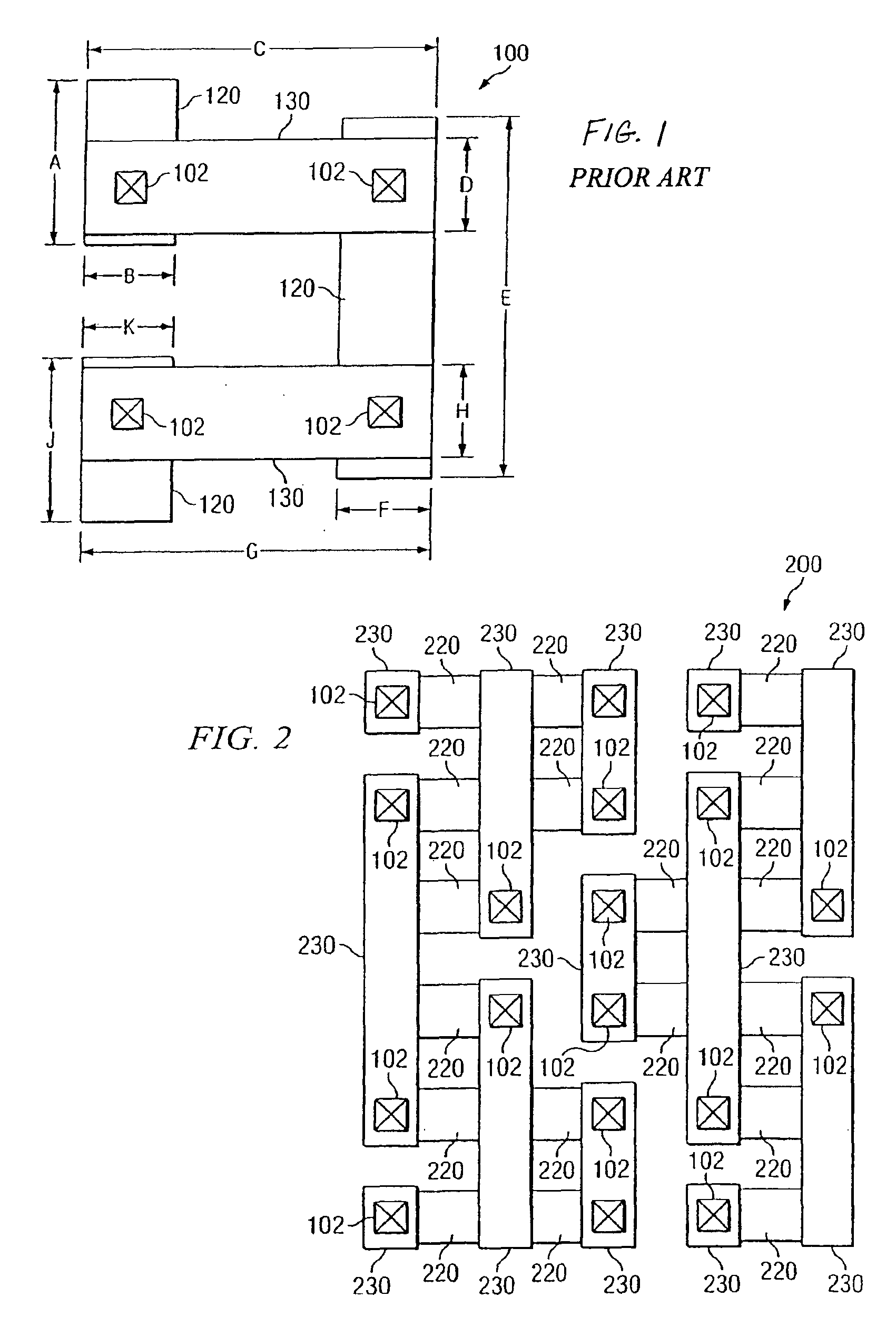
FIG. 1 diagrammatically illustrates a top down view of a semiconductor interconnect architecture (“SIA”) 100 with isolated vias 102 in accordance with the known art. In FIG. 1, lower metal layer (M1) 120 and upper metal layer (M2) 130 are interconnec...


PUM


Abstract

Thermo-mechanical stress on vias is reduced, thereby reducing related failures. This can be done by maintaining a via-to-metal area ratio at least as large as a predetermined value below which the additional stress on the vias does not significantly increase.

Description

FIELD OF THE INVENTIONThe invention relates generally to semiconductor manufacturing and, more particularly, to via density rules for semiconductor applications.BACKGROUND OF THE INVENTIONAs semiconductor wafers progress to higher density chips with shrinking geometries, the materials and processes used in wafer fabrication are changing. At the same time, each chip has literally tens of billions of electrical connections between the various metal layers and silicon devices. Electrical performance is improved though concurrent scaling of device features.Multiple conductive and insulating layers are required to enable the interconnection and isolation of devices on different layers. The interlayer dielectric (“ILD”) serves as an insulator material between each metal layer or between a first metal layer and the wafer. ILDs can be made of a low-k insulating material, such as SiLK. ILDs have many small vias, which are openings in the ILD that provide an electrical pathway from one metal ...

Claims


Application Information

Patent Timeline
IPC IPC(8): G06F17/50H01L21/768H01L23/522
CPCH01L23/5226H01L21/76816H01L2924/0002H01L2924/00
Inventor HOINKIS, MARK D.HIERLEMANN, MATTHIAS P.FAYAZ, MOHAMMED FAZILCOWLEY, ANDYKALTALIOGLU, ERDUM
Owner INFINEON TECH AG
Why Eureka
Try Eureka