Method for fabricating flip-attached and underfilled semiconductor devices

a semiconductor device and flip-attached technology, applied in the field of semiconductor devices and electronic systems, can solve the problems of delaminate the solder joint, create thermomechanical stress on its own, and eventual failure of the assembly, and achieve the effect of reducing the thermomechanical stress and simplifying the process flow

Active Publication Date: 2010-04-20
TEXAS INSTR INC
View PDF8 Cites 3 Cited by
  • Summary
  • Abstract
  • Description
  • Claims
  • Application Information

AI Technical Summary

Benefits of technology

[0006]Consequently, a need has arisen for an assembly methodology in which the stress-distributing benefits of the underfill material can be enjoyed without the deleterious side-effects of the underfilling process, resulting in enhanced device reliability. It is a technical advantage if the methodology provides an opportunity for device repair or re-working. The methodology should be coherent, low-cost, and flexible enough to be applied to different semiconductor product families and a wide spectrum of design and process variations. It is another technical advantage, if these innovations are accomplished while shortening production cycle time and increasing throughput.
[0008]Another embodiment of the invention is a semiconductor device, which comprises a workpiece with an outline and plurality of contact pads and further an external part with a plurality of terminal pads. This part is spaced from the workpiece, and the terminal pads are aligned with the workpiece contact pads, respectively. A reflow element interconnects each of the contact pads with its respective terminal pad. Thermoplastic material fills the space between the workpiece and the part; this material adheres to the workpiece, the part and the reflow elements. Further, the material has an outline substantially in line with the outline of the workpiece, and fills the space substantially without voids.
[0013]Embodiments of the present invention are related to flip-chip assemblies, ball grid array packages, chip-scale and chip-size packages, and other devices intended for reflow attachment to substrates and other external parts. It is a technical advantage that the invention offers a methodology to reduce the thermomechanical stress between the semiconductor part of a device and a substrate of dissimilar thermal expansion coefficient while concurrently controlling essential assembly parameters such as spacing between the semiconductor part and the substrate, adhesion between the parts, and selection of the temperature ranges needed in the assembly process. Additional technical advantages derive from the fact that the devices made with the thermoplastic tape are reworkable. Further, the process flow is simplified since the conventional underfill process after the flip-assembly is eliminated.

Problems solved by technology

These stresses tend to fatigue the joints and the bumps, resulting in cracks and eventual failure of the assembly.
It is well known in the industry that the temperature cycling needed for the underfill curing process can create thermomechanical stress on its own, which may be detrimental to the chip and / or the solder interconnections.
The stress created by these process steps may delaminate the solder joint, crack the passivation of the chip, or propagate fractures into the circuit structures.
In general, the sensitivity to cracking of the layered structures of integrated circuits is increasing strongly with decreasing thickness of the various layers and increasing mechanical weakness of low dielectric constant insulators.

Method used


Image

  • Method for fabricating flip-attached and underfilled semiconductor devices
  • Method for fabricating flip-attached and underfilled semiconductor devices
  • Method for fabricating flip-attached and underfilled semiconductor devices

Examples


Embodiment Construction

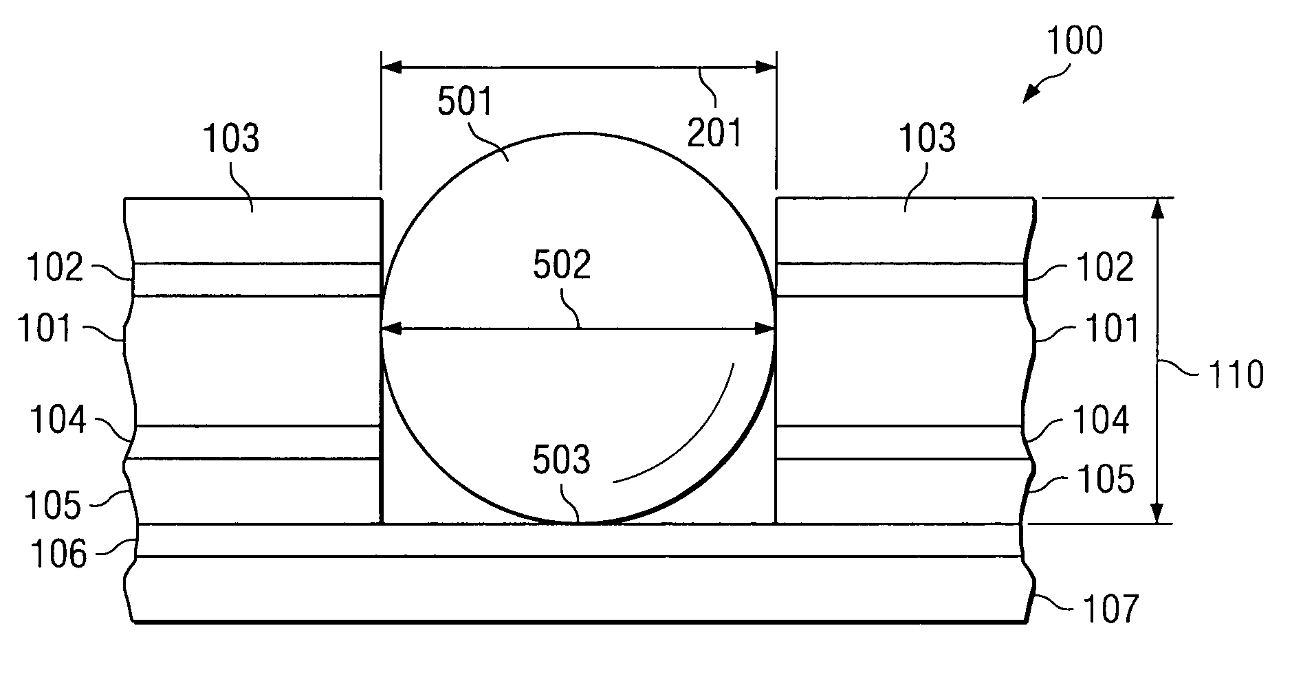
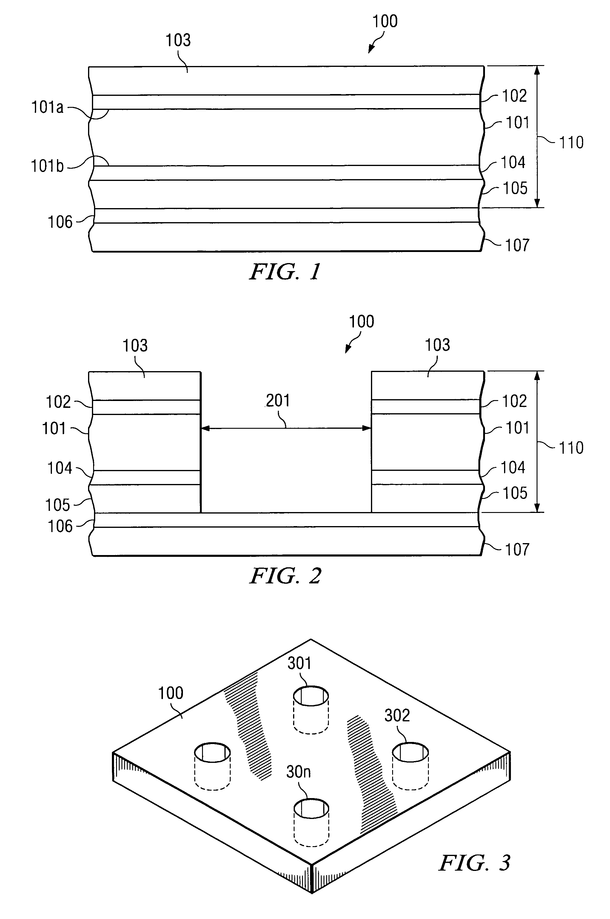
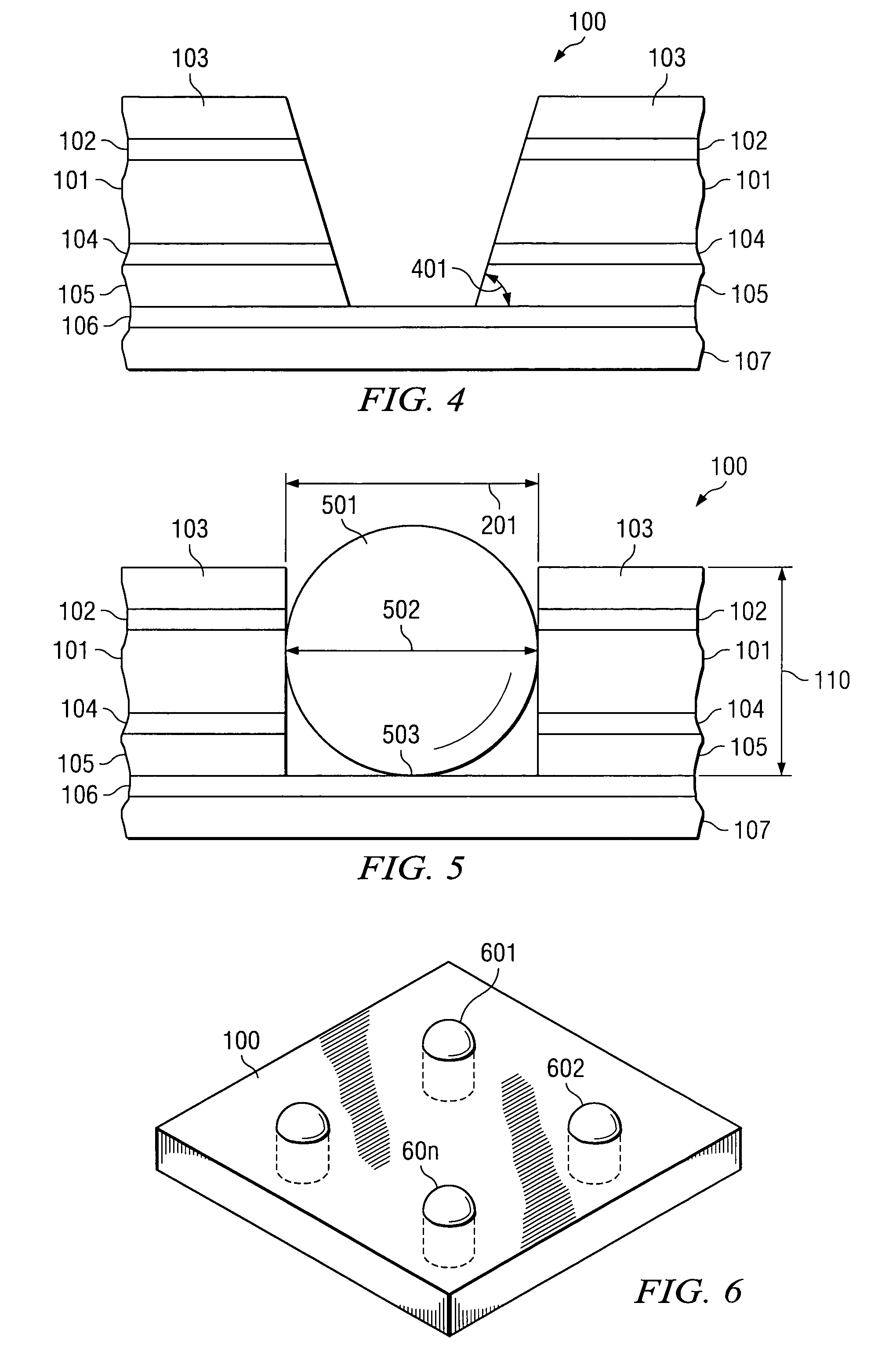
[0035]One embodiment of the invention is depicted in the schematic cross section of FIG. 1 as a tape, generally designated 100, for use as a carrier and specifically in semiconductor device assembly. Tape 100 comprises a base sheet 101 of polymeric, preferably thermoplastic material in the thickness range from about 25 to 450 μm; for some devices, the thickness may reach approximately 800 μm. Preferred thermoplastic base sheet materials include long-chain polyimides with acrylic resin or silicone resin, long-chain polyethylenes with acrylic resin, and long-chain polypropylenes with acrylic resin. The base sheet material is preferably selected so that it softens and enters the low viscosity or liquid phase in the same temperature range, which is needed for reflowing the reflow element embedded in the tape (see below). This temperature range includes, for example, the melting temperature of the solder selected for assembling the device. It is a technical advantage, when the base sheet...


PUM

PropertyMeasurementUnit
thicknessaaaaaaaaaa
thicknessaaaaaaaaaa
thicknessaaaaaaaaaa

Abstract

A semiconductor device (1700), which comprises a workpiece (1201) with an outline (1711) and a plurality of contact pads (1205) and further an external part (1701) with a plurality of terminal pads (1702). This part is spaced from the workpiece, and the terminal pads are aligned with the workpiece contact pads, respectively. A reflow element (1203) interconnects each of the contact pads with its respective terminal pad. Thermoplastic material (1204) fills the space between the workpiece and the part; this material adheres to the workpiece, the part and the reflow elements. Further, the material has an outline (1711) substantially in line with the outline of the workpiece, and fills the space (1707) substantially without voids. Due to the thermoplastic character of the filling material, the finished device can be reworked, when the temperature range for reflowing the reflow elements is reached.

Description

FIELD OF THE INVENTION[0001]The present invention is related in general to the field of electronic systems and semiconductor devices and more specifically to methods for fabricating flip-assembled and underfilled semiconductor devices.DESCRIPTION OF THE RELATED ART[0002]When an integrated circuit (IC) chip is assembled on an insulating substrate with conducting lines, such as a printed circuit motherboard, by solder bump connections, the chip is spaced apart from the substrate by a gap; the solder bump interconnections extend across the gap. The IC chip is typically a semiconductor such as silicon, silicon germanium, or gallium arsenide, the substrate is usually made of ceramic or polymer-based materials such as FR-4. Consequently, there is a significant difference between the coefficients of thermal expansion (CTE) of the chip and the substrate; for instance, with silicon (about 2.5 ppm / ° C.) as the semiconductor material and plastic FR-4 (about 25 ppm / ° C.) as substrate material, ...

Claims


Application Information

Patent Timeline
Patent Type & Authority Patents(United States)
IPC IPC(8): H01L23/48
CPCH05K3/3436H05K3/3478H01L24/29H01L21/563H01L24/81H01L2924/01015H01L2224/73104H01L2924/01032H01L2924/01033H01L2924/01047H01L2924/0105H01L2924/01075H01L2924/01082H01L2924/10329H01L2924/14H01L2924/15311H05K2201/0129H05K2201/10424H05K2201/10977H05K2203/041H01L2924/01029Y02P70/613H01L2924/181H01L2924/15787H01L2224/11334H01L2924/351H01L2224/73204H01L2924/10253H01L2924/014H01L2924/01087H01L2924/01024H01L25/105H01L2224/48091H01L2224/48227H01L2224/73203H01L2224/81101H01L2224/8121H01L2224/81815H01L2224/83101H01L2924/01002H01L2924/01005H01L2924/01006H01L2924/00014H01L2924/3512H01L2924/00H01L2224/0557H01L2224/05573H01L2224/05571H01L2224/0554Y02P70/50H01L2224/05599H01L2224/0555H01L2224/0556
Inventor WATANABE, MASAKOAMAGAI, MASAZUMI
Owner TEXAS INSTR INC
Why Eureka
Try Eureka