
Frequency multiplier and amplification circuit

a frequency multiplier and frequency technology, applied in the field of integrated circuits, can solve the problems of increasing the power consumption of the multiplier circuit, vco circuit is a complex analog device, and suffers from some significant, so as to achieve the effect of eliminating phase differences

Inactive Publication Date: 2005-03-08
XILINX INC
View PDF8 Cites 24 Cited by
  • Summary
  • Abstract
  • Description
  • Claims
  • Application Information

AI Technical Summary

Benefits of technology

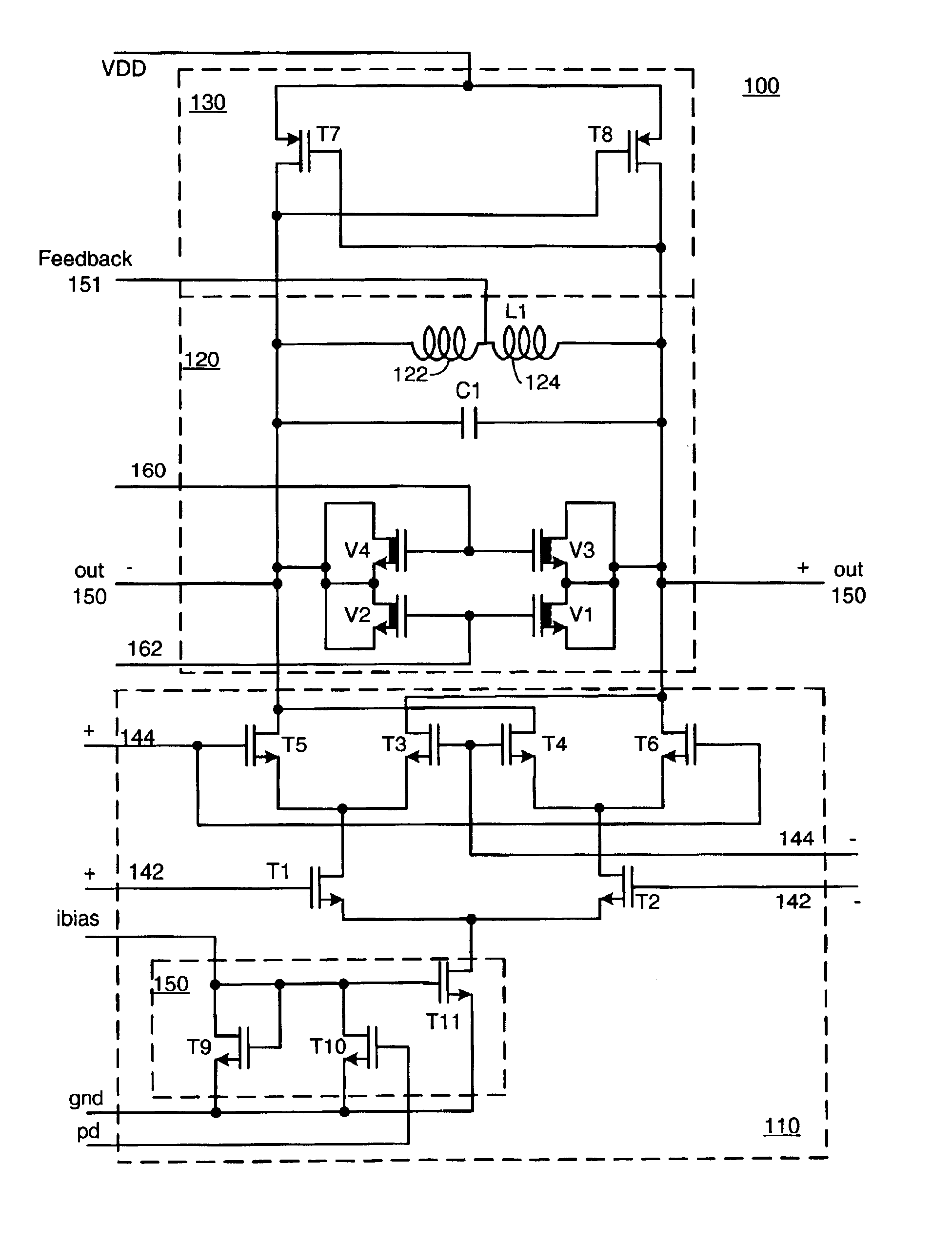
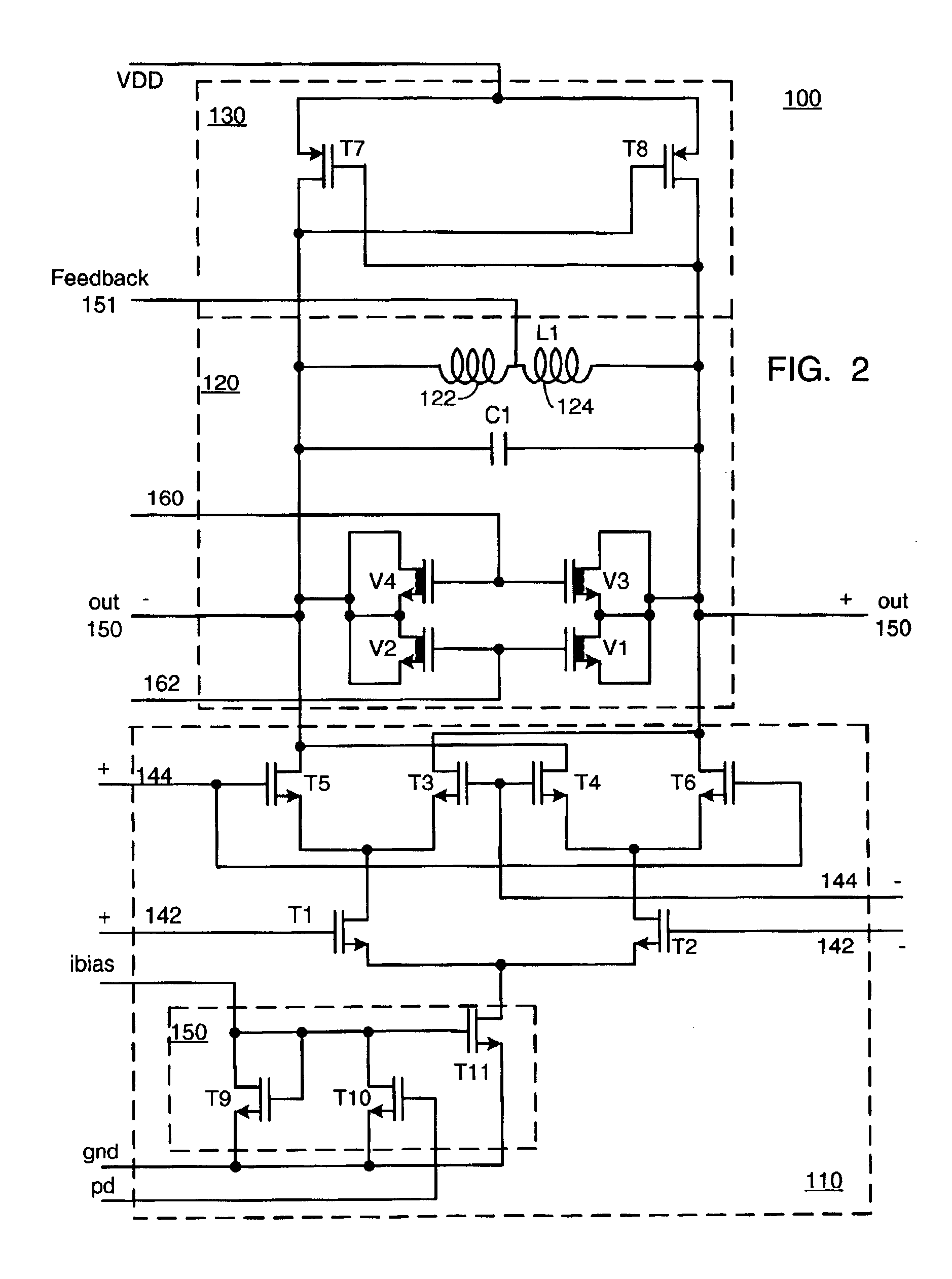
The frequency-tuned load can further comprise an inductor operably coupled to substantially attenuate the third sinusoidal waveform. Alternatively, the frequency tuned load can comprise an inductor and a capacitor, wherein the inductor is operably coupled to substantially attenuate the third sinusoidal waveform and the capacitor forms a tank frequency tuned to resonate at a frequency approximately equal to the frequency corresponding to the sum of the first and second frequencies. The frequency-tuned load can further form a bandpass filter operably coupled to substantially pass the fourth sinusoidal waveform and to substantially attenuate the third sinusoidal waveform. The frequency-tuned load can also include a tunable varactor. The frequency-tuned load can thus operate to eliminate the difference between the first and second frequencies and pass the sum of the first and second frequencies as the output of the frequency multiplier circuit, effectively removing phase differences between the frequencies being multiplied.

Problems solved by technology

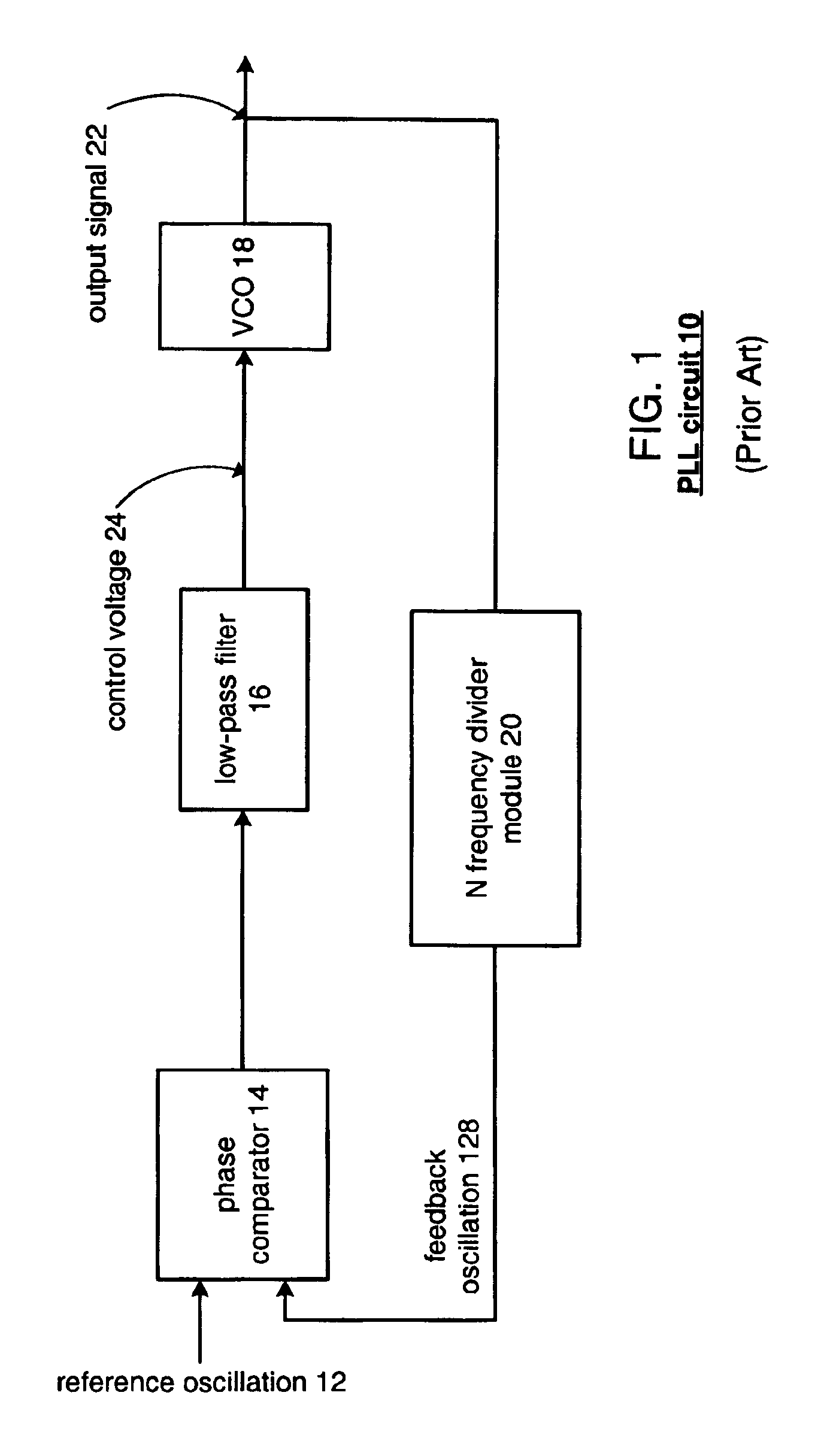
While the PLL design of FIG. 1 offers flexibility for frequency multiplication, it does suffer from some significant disadvantages.
One disadvantage of the prior art design is that the VCO operating frequency can become very high (depending on the value of N required), resulting in increased power consumption for the multiplier circuit.
Further, a VCO circuit is a complex analog device, requiring techniques for reducing power noise and frequency jitter, a common problem with PLL designs.
This solution involves not only the problems described above for PLL circuits in general, but also the increased cost associated with the additional circuit real estate needed for the additional PLL circuit.
The use of multiple PLL circuits is thus not a desired solution because of cost and complexity.
As a result, prior art frequency multiplication circuits are complex and costly, and require additional techniques for reducing power noise and frequency jitter.

Method used


Image

  • Frequency multiplier and amplification circuit
  • Frequency multiplier and amplification circuit
  • Frequency multiplier and amplification circuit

Examples


Embodiment Construction

In general, the embodiments of the present invention provide a low jitter frequency multiplier without the need for a PLL circuit. Such a frequency doubler has wide applications in communications systems. The embodiments of this invention provide an integrated circuit with the ability to directly use the same differential signal to perform frequency multiplication. The present invention further provides the ability to drive a large load with the addition of a switchable bandpass filtering boosting amplifier at the output of the frequency multiplier circuit.

Unlike the prior art, the embodiments of this invention base their operation on using the same reference signal to perform frequency multiplication, thus eliminating the required 90 degree phase shift of the prior art. The present invention accomplishes this by using the equivalence:

Cos(2θ)=1−2(Sin θ)2  Equation 1

Rearranging Equation 1 yields:

Sin(θ)*Sin(θ)=(1−Cos(2*θ)) / 2  Equation 2

Based on Equation 2, the embodiments of this i...


PUM


Abstract

A frequency multiplier and amplification circuit are disclosed. One embodiment of the present invention comprises: a multiplier operably coupled to multiply a first sinusoidal waveform having a first frequency with a second sinusoidal waveform having a second frequency to produce a third sinusoidal waveform, having a frequency representative of a difference between the first frequency and the second frequency, and a fourth sinusoidal waveform having a frequency representative of a sum of the first and second frequencies; and a frequency-tuned load operably coupled to substantially attenuate the third sinusoidal waveform and to substantially pass the fourth sinusoidal waveform as an output of the frequency-tuned multiplier circuit. The frequency-tuned multiplier circuit can be a single-ended multiplier circuit or a differential multiplier circuit with corresponding single-ended or differential first and second sinusoidal waveforms.

Description

TECHNICAL FIELD OF THE INVENTIONThis invention relates generally to integrated circuits and, more particularly, to a frequency multiplier for use in such integrated circuits. Even more particularly, the present invention relates to a frequency multiplier and amplification circuit that is not based on a phase-locked loop.BACKGROUND OF THE INVENTIONPhase-locked loop (“PLL”) circuits are well known in the art and are often used for frequency multiplication. As shown in FIG. 1, the main components of a PLL circuit 10 for multiplying a reference signal 12's frequency by N comprise a phase comparator 14, a low-pass filter 16, a voltage control oscillator (“VCO”) 18 and an N frequency divider module 20. The N frequency divider module 20 provides feedback control to provide a correct frequency comparison with the reference signal 12 in the phase comparator 14. The N frequency divider module 20 supplies the phase comparator 14 with a feedback signal obtained by N-dividing an output signal 22...

Claims


Application Information

Patent Timeline
IPC IPC(8): H03J3/00H03J3/20H03D7/14
CPCH03D7/1441H03J3/20H03D7/1475H03D7/1483H03D7/1458H03D2200/0033
Inventor LU, JINGHUI
Owner XILINX INC
Learn More