Method of fabricating an ESD device on SOI

a technology of silicon dioxide and soi, which is applied in the direction of semiconductor devices, electrical equipment, transistors, etc., can solve the problems of buried oxide layer 14/b> tending to display excessive heating, detrimental effect of soi esd protection on manufacturers, and inability to meet the requirements of esd protection, etc., to achieve the effect of improving the esd performance of soi transistors

Inactive Publication Date: 2005-03-15
TAIWAN SEMICON MFG CO LTD
View PDF31 Cites 19 Cited by
  • Summary
  • Abstract
  • Description
  • Claims
  • Application Information

AI Technical Summary

Benefits of technology

A principal object of the present invention is to provide an effective and very manufacturable method for improving the ESD performance of an SOI transistor.

Problems solved by technology

However, ESD protection of SOI devices remains a significant challenge to manufacturers.
However, the presence of the buried oxide layer 14 may have detrimental effects for the ESD performance of the device.
Therefore, the buried oxide layer 14 tends to display excessive heating due to current flow.
In addition, the absence of a bulk current path causes current concentration near the surface of the MOS channel where excessive energy dissipation can cause damage.

Method used


Image

  • Method of fabricating an ESD device on SOI
  • Method of fabricating an ESD device on SOI
  • Method of fabricating an ESD device on SOI

Examples


Embodiment Construction

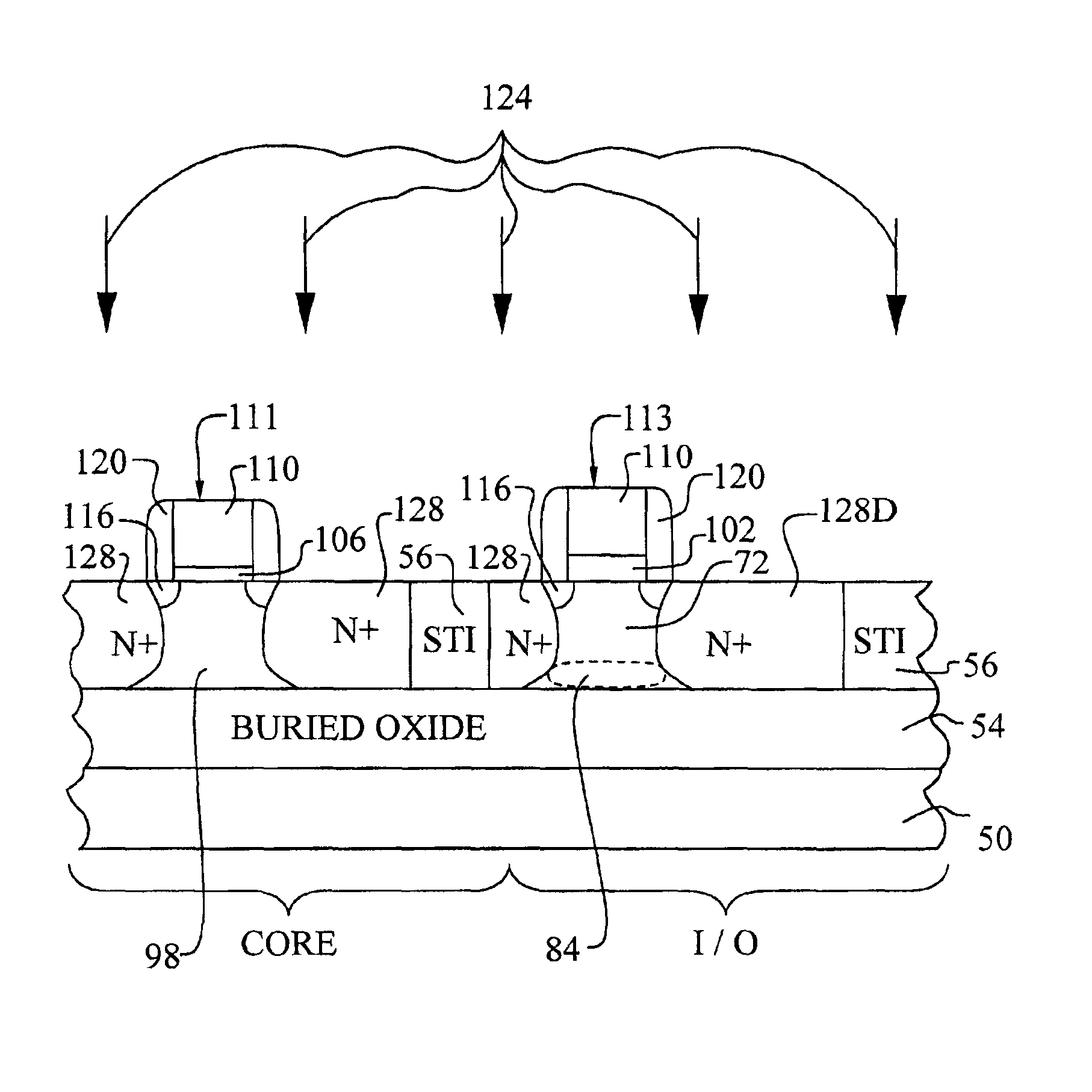
The preferred embodiments of the present invention disclose a method to form a SOI MOSFET device having improved ESD performance. A higher concentration region is formed in the body of the MOSFET to reduce the drain-to-body reverse breakdown voltage. The method is useful for either NMOS or PMOS devices. The method is especially useful to improve ESD current uniformity in interleaved, or multi-finger devices. It should be clear to those experienced in the art that the present invention can be applied and extended without deviating from the scope of the present invention.

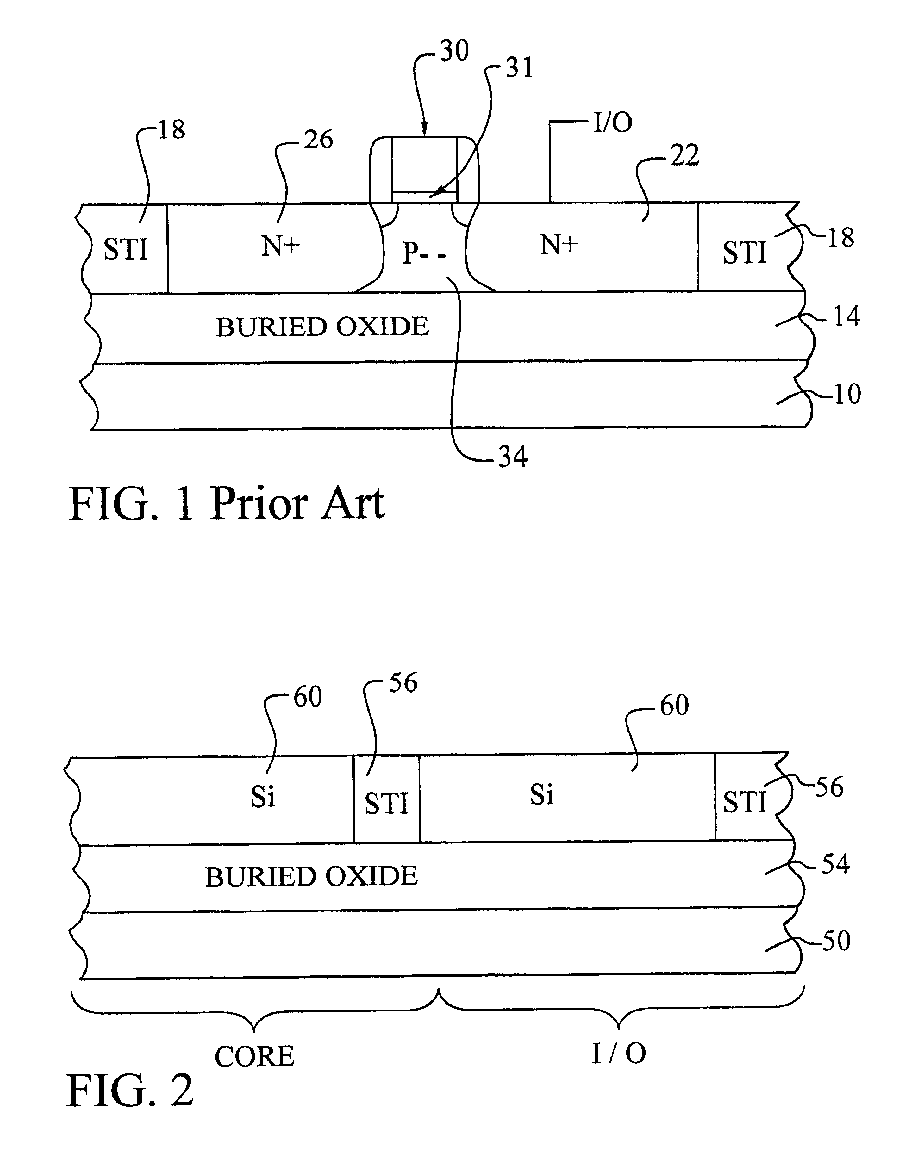
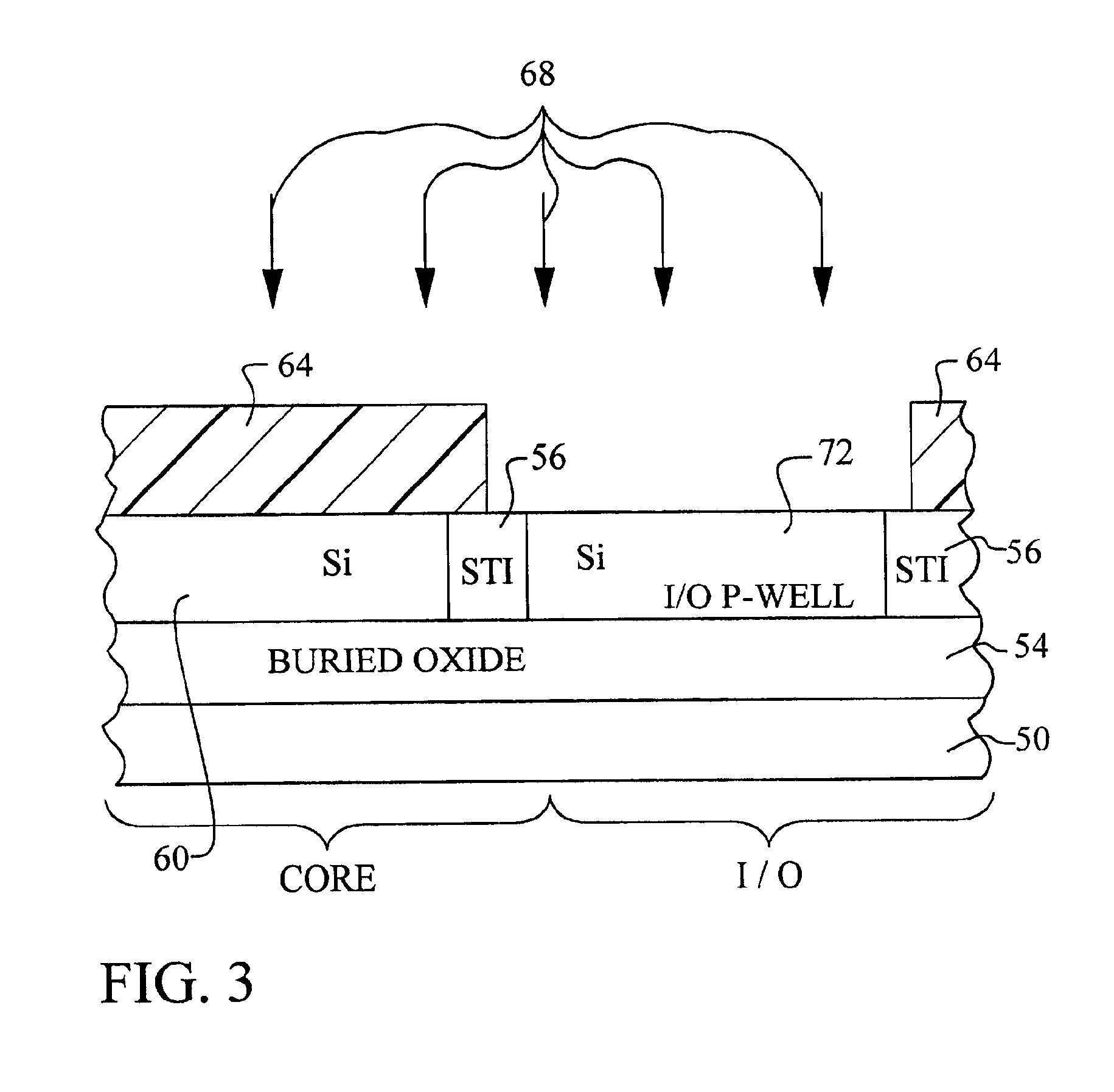
Referring now to FIG. 2, the preferred starting point of the method the present invention is shown. The present invention applies to any SOI system. In this case, the SOI system, shown in cross-sectional representation, comprises a buried oxide layer 54 overlying a substrate 50. For example, the substrate 50 may comprise silicon. The buried oxide layer 54, in this case preferably comprises a thick silicon oxide layer ...


PUM


Abstract

A method to form transistors having improved ESD performance in the manufacture of an integrated circuit device is achieved. The method includes providing a SOI substrate with a doped silicon layer and a buried oxide layer. The doped silicon layer has a first conductivity type and overlies the buried oxide layer. Ions are implanted into the SOI substrate to form higher concentration regions in the doped silicon layer. The higher concentration regions have the first conductivity type and are formed substantially below the top surface of the doped silicon layer. MOS gates are formed. These MOS gates include an electrode layer overlying the doped silicon layer with a gate oxide layer therebetween. Source and drain regions are formed in the doped silicon layer to complete the transistors in the manufacture of the integrated circuit device. The source and drain regions contact the higher concentration regions and have a second conductivity type.

Description

BACKGROUND OF THE INVENTION(1) Field of the InventionThe invention relates to silicon-on-insulator (SOI) devices and, more particularly, to a method to form a SOI device having improved ESD performance.(2) Description of the Prior ArtAt present, the vast majority of integrated circuit products are formed on bulk semiconductor wafers. However, silicon-on-insulator (SOI) wafer-based products are under development as a majority technology for the future. SOI offers the advantages of improved short channel performance, improved isolation, and reduced power supply capability. However, ESD protection of SOI devices remains a significant challenge to manufacturers.Referring now to FIG. 1, an example of a prior art SOI MOSEET is shown. The SOI substrate comprises a buried oxide layer 14, typically many microns thick, that is formed overlying a substrate 10. A silicon layer is formed overlying the buried oxide layer 14. In this case, the silicon layer has been doped to form an N+ source 26, ...

Claims


Application Information

Patent Timeline
Patent Type & Authority Patents(United States)
IPC IPC(8): H01L29/786H01L21/02H01L29/66H01L21/336H01L27/02
CPCH01L29/78621H01L29/78612H01L29/66772H01L27/0251
Inventor YU, TA-LEE
Owner TAIWAN SEMICON MFG CO LTD
Why Eureka
Try Eureka