Confocal wafer inspection method and apparatus using fly lens arrangement

a technology of confocal wafers and inspection methods, applied in the direction of lenses, instruments, optical elements, etc., can solve problems such as severe signal variations, and achieve the effect of reducing the risk of signal variation, reducing the risk of optical damage, and improving the accuracy of inspection results

Inactive Publication Date: 2005-03-15
KLA CORP
View PDF46 Cites 47 Cited by
  • Summary
  • Abstract
  • Description
  • Claims
  • Application Information

AI Technical Summary

Benefits of technology

One potential use of the system is in conjunction with a slit laser confocal arrangement. Also, the system may employ autofocus capabilities which must be kept stable for particular wafer specimens. Unstable autofocus may tend to cause severe signal variations and is generally unusable. In particular, the autofocus used in the present system ignores various layers rather than evaluating multiple confocal measurements and cancelling undesirable measurements. The process of ignoring layers not pertient to the scan is that focus is more rapid and effective for multiple height measurements.
If the system uses a large NA (numerical aperture) objective, high angle darkfield can be employed in the system by using an aperture in a fourier plane. Confocal Z discrimination, inherent in confocal systems, reduces the necessity for providing both high angle of incidence and grazing angle dark field evaluation. In such a high angle dark field arrangement, the binary fly lens arrangement permits constructing efficient, directional dark field spots for confocal imaging.
An alternate embodiment of the current invention is to use an AOD scanning system, which provides better mechanical stability over a mechanical polygon scanning system. This increases the stability provided by the fixed array of conjugate pinholes in the illumination and collection paths of the system.

Problems solved by technology

Unstable autofocus may tend to cause severe signal variations and is generally unusable.

Method used


Image

  • Confocal wafer inspection method and apparatus using fly lens arrangement
  • Confocal wafer inspection method and apparatus using fly lens arrangement
  • Confocal wafer inspection method and apparatus using fly lens arrangement

Examples


Embodiment Construction

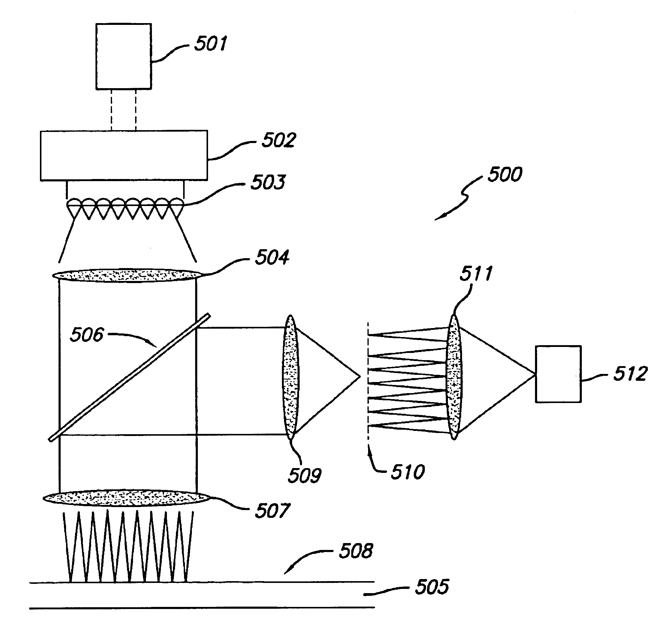
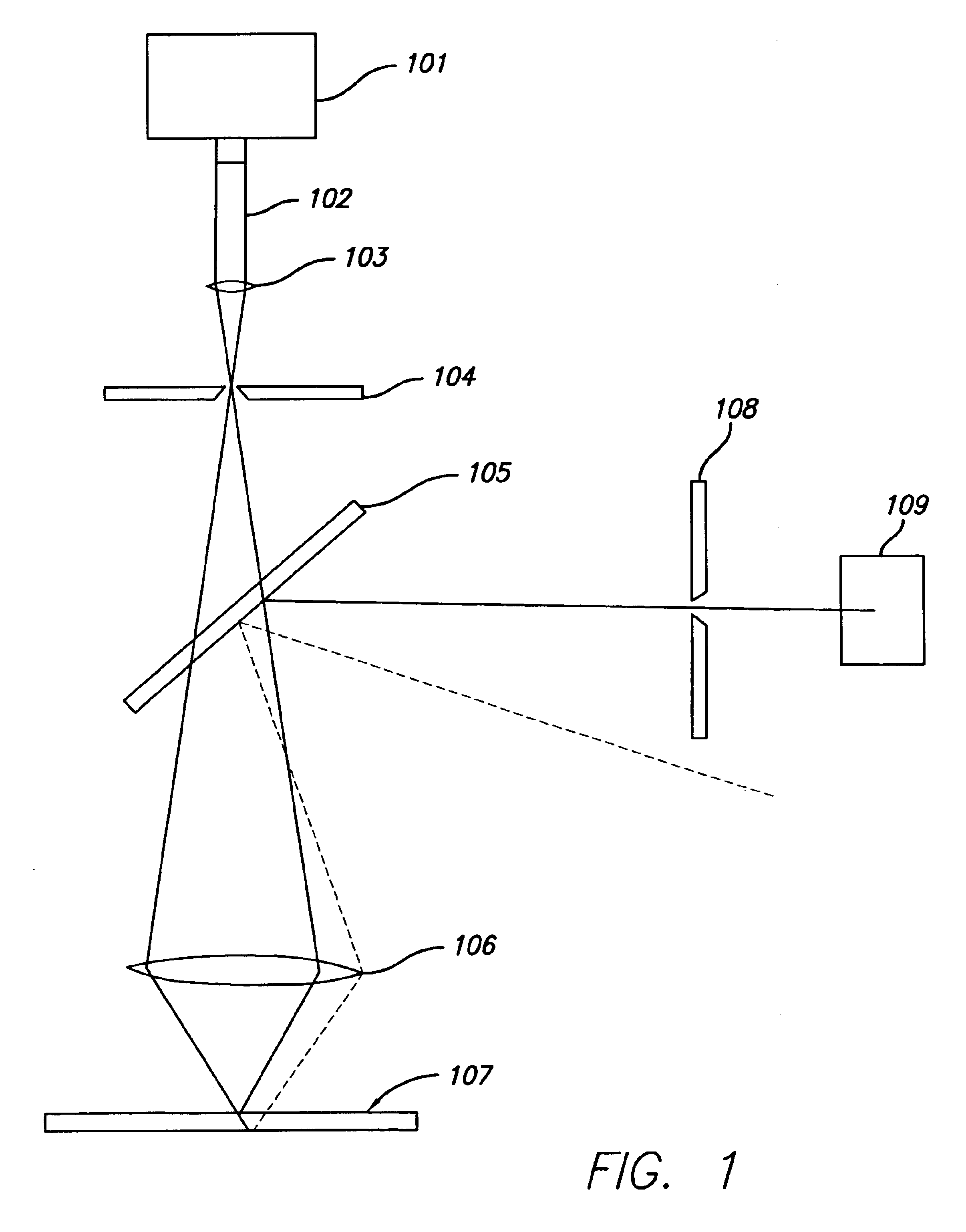
The inventive system disclosed herein employs multiple wavelength confocal inspection techniques in conjunction with an offset fly lens arrangement and a TDI CCD sensor. Multiple wavelength confocal inspection enhances the ability to obtain an extended focus image or enhanced surface profile information with a single scan, or the ability to scan at varying specimen depths while maintaining focus on the various depths during a single scan pass. The use of such techniques provides light to be transmitted at multiple wavelengths without crosstalk.

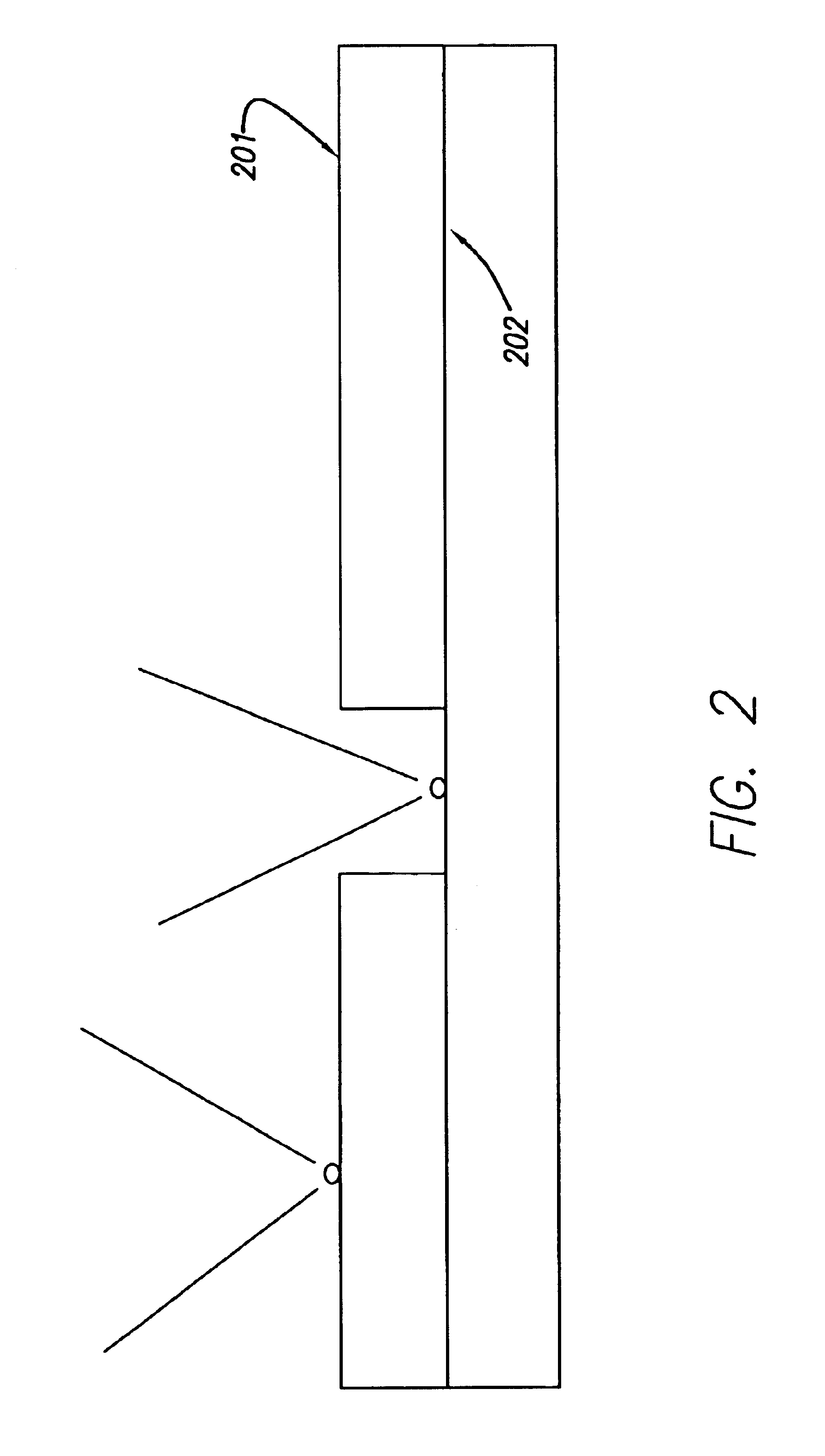
FIG. 2 illustrates a multilevel specimen which benefits confocal inspection. A first scan frequency provides a focused image based on the topmost surface 201 of the specimen, while a second scan frequency provides a focused image based on a contact bottom 202 of the specimen. A further third scan frequency, not shown, provides a focused image based on the bottom surface of the specimen.

The three returns from the scan of the specimen illustrate...


PUM


Abstract

A semiconductor wafer inspection system and method is provided which uses a multiple element arrangement, such as an offset fly lens array. The preferred embodiment uses a laser to transmit light energy toward a beam expander, which expands the light energy to create an illumination field. An offset fly lens array converts light energy from the illumination field into an offset pattern of illumination spots. A lensing arrangement, including a first lens, a transmitter / reflector, an objective, and a Mag tube imparts light energy onto the specimen and passes the light energy toward a pinhole mask. The pinhole mask is mechanically aligned with the offset fly lens array. Light energy passing through each pinhole in the pinhole mask is directed toward a relay lens, which guides light energy onto a sensor. The offset fly lens array corresponds to the pinhole mask. The offset pattern of the offset fly lens array is chosen such that spots produced can be recombined into a continuous image, and the system utilizes a time delay and integration charge coupled device for rapid sensing along with an autofocus system that measures and cancels topological features of the specimen.

Description

BACKGROUND OF THE INVENTION1. Field of the InventionThe present invention relates generally to precision optical inspection methods for specimens such as semiconductor wafers, and more specifically to a method and apparatus for performing microscopic inspection and measurement of integrated circuit wafer geometries using laser confocal microscopy.2. Description of the Related ArtIn integrated circuit inspection, particularly inspection of semiconductor wafers or photomasks from which such circuits are fabricated, different methods have been employed to address particular characteristics of the wafers or advantages afforded by specific inspection technologies.One such method that has previously been employed in semiconductor wafer or photomask inspection is confocal microscopy. Confocal imaging entails suppressing out of focus specimen elements at image formation. The suppression of out of focus elements occurs partially as a result of the specimen not being illuminated and imaged as...

Claims


Application Information

Patent Timeline
Patent Type & Authority Patents(United States)
IPC IPC(8): G02B21/00
CPCG01N21/9501G02B3/0056G02B27/40G02B21/0024G02B21/0028G02B21/008
Inventor FAIRLEY, CHRISTOPHER R.FU, TAO-YITSAI, BIN-MING BENJAMINYOUNG, SCOTT A.
Owner KLA CORP
Why Eureka
Try Eureka