Method for producing silicon single crystal having no flaw

a single crystal, defect-free technology, applied in the direction of crystal growth process polycrystalline material growth, etc., can solve the problems of inability to produce defect-free crystals (perfect crystals), slight decrease in uniformity, and inability to actually be practical

Inactive Publication Date: 2005-03-22
SUMCO TECHXIV
View PDF5 Cites 37 Cited by
  • Summary
  • Abstract
  • Description
  • Claims
  • Application Information

AI Technical Summary

Problems solved by technology

Still, this only refers to the maximum permissible range, and is not actually practical.
This means that slight decreases the uniformity of G make it essentially impossible to produce defect-free crystals (perfect crystals).
Because of this, with the method proposed in Publication 1, even if crystals are pulled up at the same pull-up rate, heater output and so forth, defect-free crystals will sometimes be obtained and sometimes not, meaning that the production of defect-free crystals will be extremely unstable.
Furthermore, the following two problems are encountered with the proposal in Publication 1.[1] G (the average temperature gradient within a crystal in the axial direction) is hard to evaluate and difficult to predict.[2] G varies during pull-up.
Specifically, factors that cause G to vary during pull-up include changes in the thermal balance resulting from a change in the length of the crystal, changes in the thermal balance resulting from a change in the relative positions of the crucible and heater, and changes in the amount of melt, and it is difficult to ascertain and control these.
Also, whereas the growth

Method used


Image

  • Method for producing silicon single crystal having no flaw
  • Method for producing silicon single crystal having no flaw
  • Method for producing silicon single crystal having no flaw

Examples


Embodiment Construction

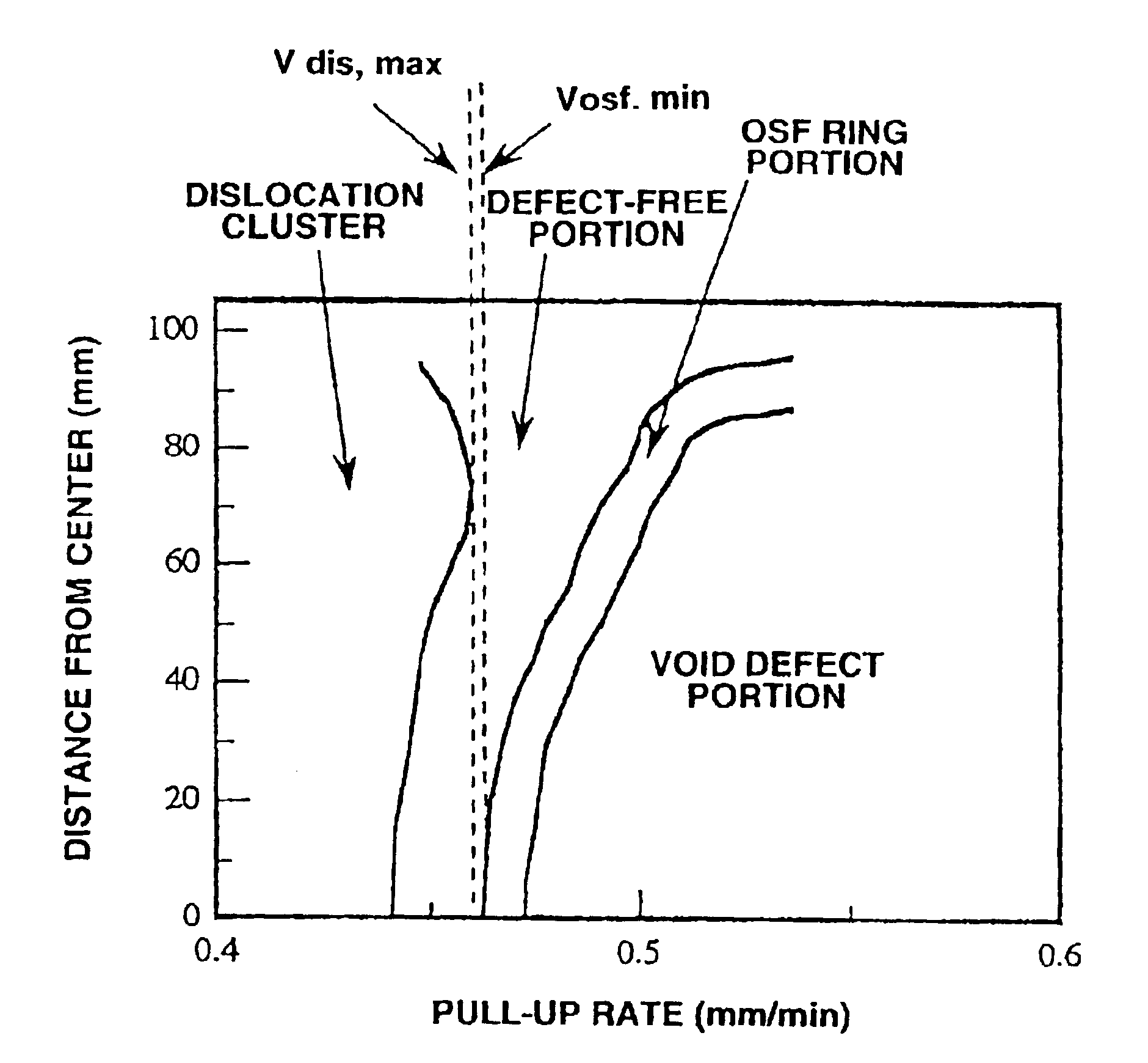
As discussed above, defect-free crystals are obtained by controlling the solid-liquid interface height and the temperature gradient on the crystal side face to the proper state. It is well known that the temperature gradient on the crystal side face can be adjusted by adjusting the radiation environment to which the crystal side face are subjected. As to the adjustment of the solid-liquid interface height, however, a numerical evaluation of the situation is difficult. Nevertheless, the factors that control this, and the qualitative tendencies of the action thereof, are clear, and the right control conditions can be found by a certain amount of trial and error.

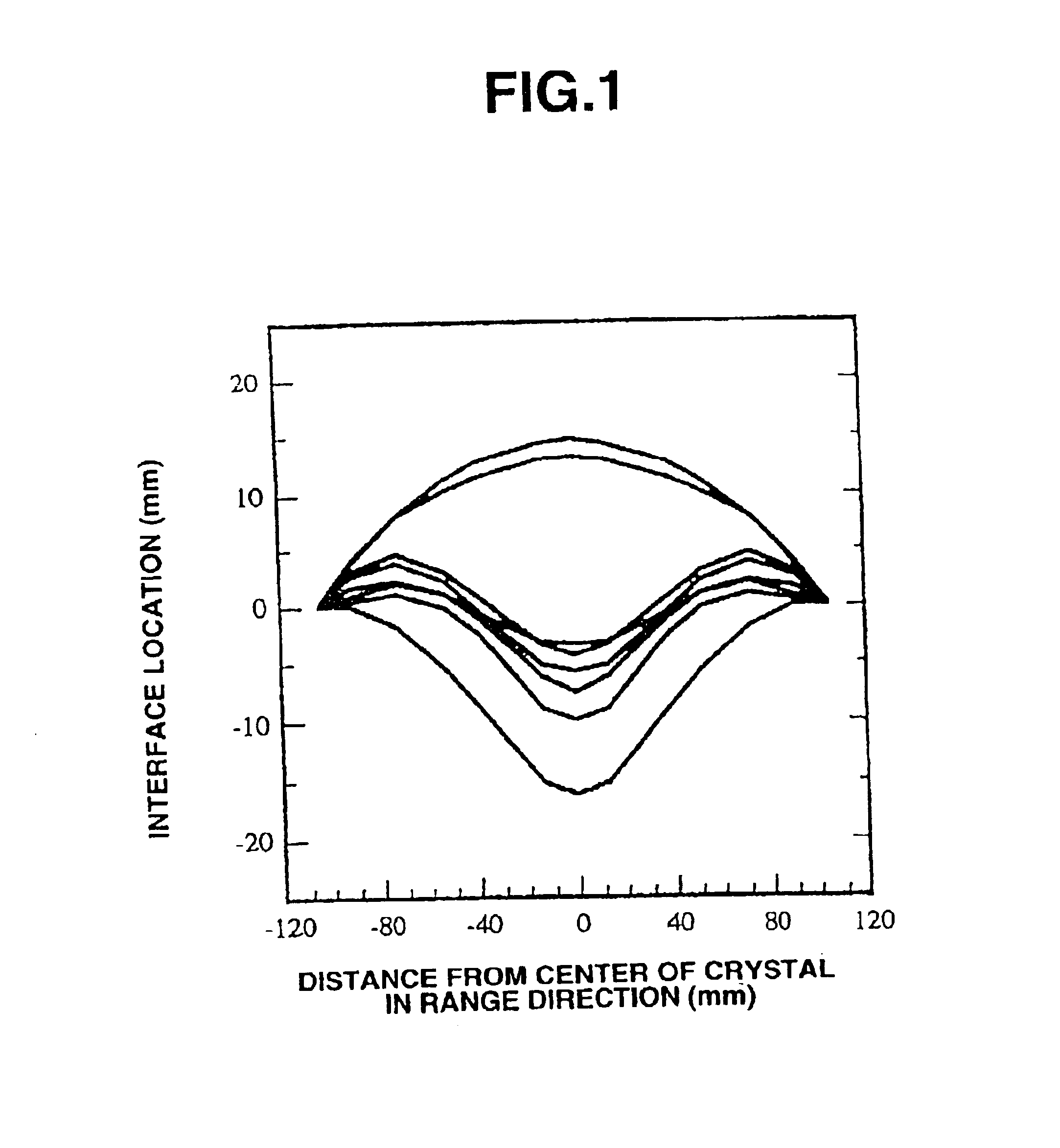
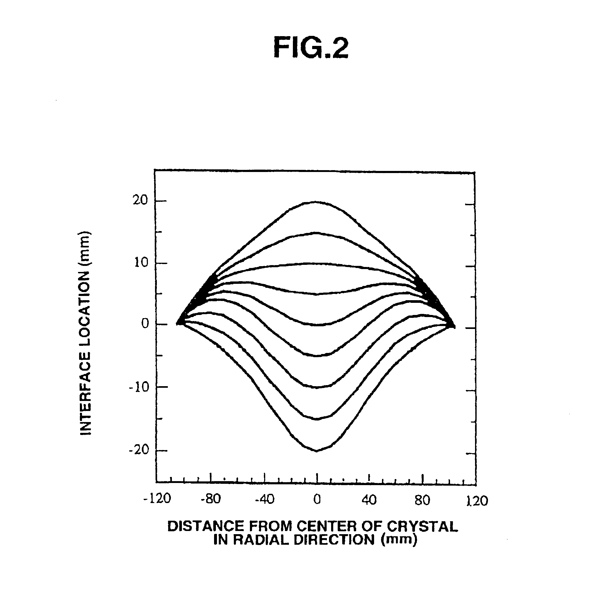
Examples of controlling the height of the solid-liquid interface will now be given. FIGS. 14, 15, and 16 show how the height of the solid-liquid interface is related to the crystal rotational speed per unit of time, the crucible rotational speed per unit of time, and the strength of the applied lateral magnetic field, respectiv...


PUM


Abstract

A method for producing a silicon ingot having no defect over a wide range of region with stability and good reproducibility, wherein when a silicon single crystal (11) is pulled up form a silicon melt (13), the shape of a solid-liquid interface (14) which a boundary between the silicon melt (13) and the silicon single crystal (11) and the temperature distribution on the side face (11b) of a single crystal under being pulled up are appropriately controlled.

Description

TECHNICAL FIELDThis invention relates to a method for producing defect-free crystals (defect-free silicon single crystals), and to a silicon single crystal produced by this method.BACKGROUND ARTAs semiconductor devices have been finer and more highly integrated in recent years, there has been an increasing need for silicon wafers of higher quality. This also underscores the need to reduce crystal defects that occur in the course of producing silicon single crystals.[Defects Contained in Single Crystals and Behavior thereof]It has been understood that the following three types of crystal defect are commonly included in single crystals and related to deterioration of the performances of a device.[1] Void defects thought to occur through the agglomeration of vacancies[2] Oxidation induced stacking faults (OSF)[3] Dislocation clusters thought to occur through the agglomeration of interstitial siliconIt is known that the way these defects occur varies as follows with the growth condition...

Claims


Application Information

Patent Timeline
IPC IPC(8): C30B15/22C30B15/20C30B15/14C30B15/00C30B29/06H01L21/208
CPCC30B15/14C30B15/203C30B29/06Y10T117/1004Y10T117/1008Y10T117/1068C30B15/00
Inventor NAKAMURA, KOZOSAISHOJI, TOSHIAKITOGAWA, SHINJIKOTOOKA, TOSHIROUMAEDA, SUSUMU
Owner SUMCO TECHXIV
Why Eureka
Try Eureka