
High efficiency light emitting diode and method of making the same

a light-emitting diode, high-efficiency technology, applied in the direction of semiconductor/solid-state device manufacturing, semiconductor devices, electrical devices, etc., can solve the problems of low thermal conductivity of gaas substrate b>1/b>, small external quantum efficiency of this kind of conventional algainp led, and many disadvantages of conventional technology, etc., to achieve high efficiency

Inactive Publication Date: 2005-03-22
EPISTAR CORP
View PDF8 Cites 191 Cited by
  • Summary
  • Abstract
  • Description
  • Claims
  • Application Information

AI Technical Summary

Benefits of technology

The present invention provides a high efficiency light emitting diode. The light emitting diode comprises an LED epitaxial structure which has a plurality of III-V compound semiconductor layers grown on a lattice matched substrate and can generate light in responsive to injection current, a metal reflector composed of

Problems solved by technology

Therefore, the external quantum efficiency of this kind of conventional AlGaInP LED is small.
Besides, the thermal conductivity of GaAs is only about 44 W / m-° C. The low thermal conductivity of the GaAs substrate 1 is not good enough to dissipate the heat generated.
However, those conventional technologies still have several disadvantages and limitations.
The DBR layer 2 can only effectively reflect the light vertically emitted towards the GaAs substrate 1, so that the improvement of external quantum efficiency is limited.
However, the fabrication process of the TS AlGaInP LED is too complicated.
Therefore, it is difficult to manufacture these TS AlGaInP LEDs in high yield and low cost.
These hillocks can result in incomplete bonding regions while the LED epi-layers portion 20 bonds with the supporting substrate 30 these regions will be problematic and present deteriorated performance of LED chips.

Method used


Image

  • High efficiency light emitting diode and method of making the same
  • High efficiency light emitting diode and method of making the same
  • High efficiency light emitting diode and method of making the same

Examples


Embodiment Construction

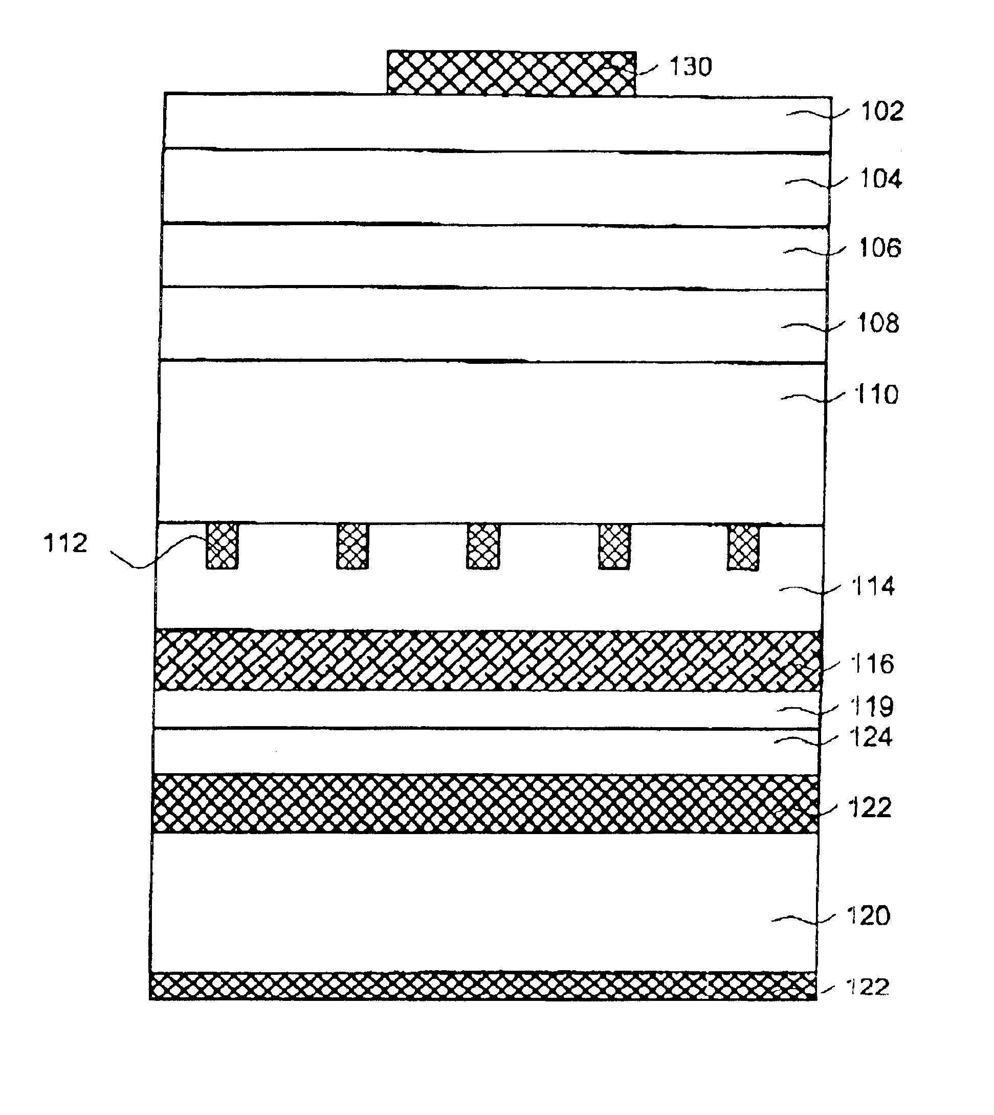
As described above, the conventional AlGaInP LEDs have many disadvantages, and thus the present invention provides a newly LED structure which comprises a transparent conductive oxide layer in between metal reflector layer and the upper side of light emitting structure solve those disadvantages present in conventional LEDs and will be described in detail as below.

Referring to FIG. 6A, an epitaxial structure 118 of a light emitting structure is consisted of a temporary GaAs substrate 100, an etching stop layer 102, an n-type (AlxGa1-x)0.5In0.5P lower cladding layer 104 with an Al composition of about 50%-100%, an (AlxGa1-x)0.5In0.5P active layer 106 with an Al composition of about 0%-45%, a p-type (AlxGa1-x)0.5In0.5P upper cladding layer 108 with an Al composition of about 50%-100%, a p-type ohmic contact layer 110.

The material of the etching stop layer 102 can be selected from any III-V compound semiconductor material that has a lattice matched with that of the GaAs substrate 100. T...


PUM


Abstract

A high efficiency light emitting diode (LED) with metal reflector and the method of making the same is disclosed. The metal reflector is composed of at least two layers with one transparent conductive layer and the other highly reflective metal layer. The transparent conductive layer allows most of the light passing through without absorption and then reflected back by the highly reflective metal layer. The transparent conductive layer is selected from one of the materials that have very little reaction with highly reflective metal layer even in high temperature to avoid the reflectivity degradation during the chip processing. With this at least two layer metal reflector structure, the light emitting diode with vertical current injection can be fabricated with very high yield.

Description

BACKGROUND OF THE INVENTION1. Field of the InventionThe present invention relates to a high efficiency light emitting device, and more particularly to a III-V compound semiconductor light emitting diode with a highly reflective metal reflector therein to avoid the light absorption by the substrate.2. Description of the Prior ArtThe conventional AlGaInP LED, as shown in FIG. 1, has a double heterostructure (DH), which is consisted of an n-type (AlxGa1-x)0.5In0.5P lower cladding layer 3 with an Al composition of about 70%-100%, formed on an n-type GaAs substrate 1, an (AlxGa1-x)0.5In0.5P active layer 5 with an Al composition of 0%-45%, a p-type (AlxGa1-x)0.5In0.5P upper cladding layer 7 with an Al composition 70%-100% and a p-type high energy bandgap current spreading layer 9 such as layers of GaP, GaAsP, AlGaAs or ZnO. However, the portion of the light emits from the active layer 5 towards the substrate will be totally absorbed by GaAs substrate 1. Therefore, the external quantum eff...

Claims


Application Information

Patent Timeline
IPC IPC(8): H01L33/00H01L33/40H01L33/46
CPCH01L33/46H01L33/405
Inventor CHEN, TZER-PERNG
Owner EPISTAR CORP
Features
  • Generate Ideas
  • Intellectual Property
  • Life Sciences
  • Materials
  • Tech Scout
  • Unparalleled Data Quality
  • Higher Quality Content
  • 60% Fewer Hallucinations
Learn More