Process for manufacturing a semiconductor wafer integrating electronic devices and a structure for electromagnetic decoupling

a semiconductor wafer and electronic device technology, applied in semiconductor/solid-state device manufacturing, solid-state devices, electric devices, etc., can solve the problems of electromagnetic coupling with the substrate, increase in overall power dissipation, and limitations of fabrication processes currently available, so as to improve electromagnetic decoupling

Inactive Publication Date: 2005-03-22
STMICROELECTRONICS SRL
View PDF43 Cites 78 Cited by
  • Summary
  • Abstract
  • Description
  • Claims
  • Application Information

AI Technical Summary

Benefits of technology

An embodiment of the present invention provides a process for manufacturing a semiconductor w

Problems solved by technology

These capacitances and mutual parasitic inductances, in fact, alter the characteristics of the devices and lead to an increase in the overall power dissipation.
In addition, the problem of electromagnetic coupling with the substrate is particularly significant in the case of pure passive components, i.e., of those components that are designed to have a behavior of an exclusively capacitive, inductive, or resistive type in a wide frequency band.
However, the fabrication processes currently available present limits which, in practice, do not enable formation of dielectric layers having satisfactory characteristics of insulation.
In this case, however, the time required for carrying out the oxidation step is extremely long, on account of the low diffusiveness of the reagents, and the process is too slow to be exploited at an industrial level.
Alternatively, it has been proposed to use thick layers of deposited oxide, which can be made in slightly shorter times. However, the improvement that is obtained is not yet sufficient and, moreover, the dielectric characteristics of the deposited oxide are inferior to those of the thermal oxide.
SOI wafers first of all present the disadvantage of being very costly, in so far as their preparation requires the use of complex processes; in the second

Method used


Image

  • Process for manufacturing a semiconductor wafer integrating electronic devices and a structure for electromagnetic decoupling
  • Process for manufacturing a semiconductor wafer integrating electronic devices and a structure for electromagnetic decoupling
  • Process for manufacturing a semiconductor wafer integrating electronic devices and a structure for electromagnetic decoupling

Examples


Embodiment Construction

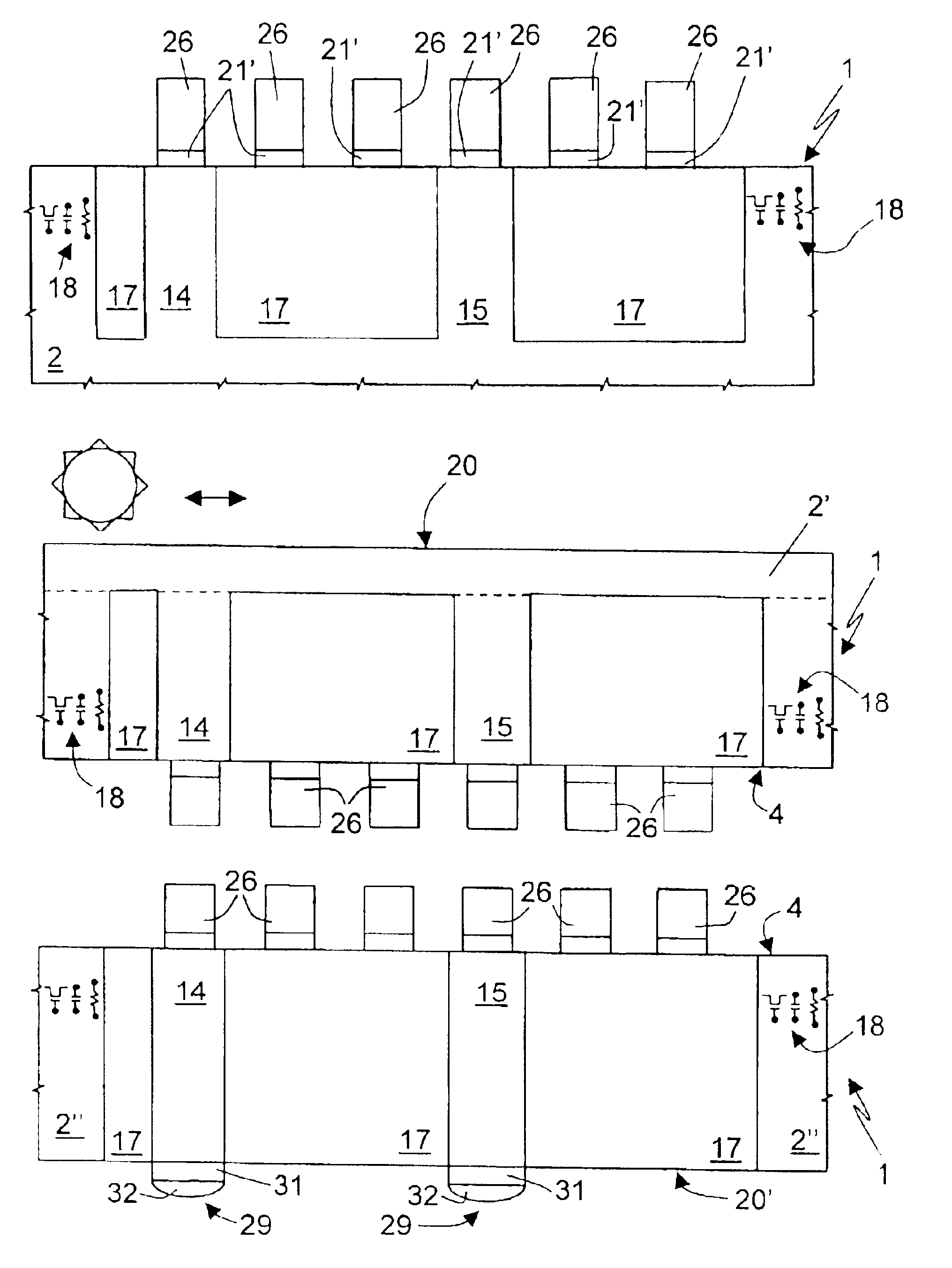
In the embodiment described hereinafter, the process that forms the subject of the present invention is used for the fabrication of an inductor with a high figure of merit. This must not, however, be considered in any way limiting, since the process can be advantageously used for the fabrication of devices of various kinds, whether active or passive.

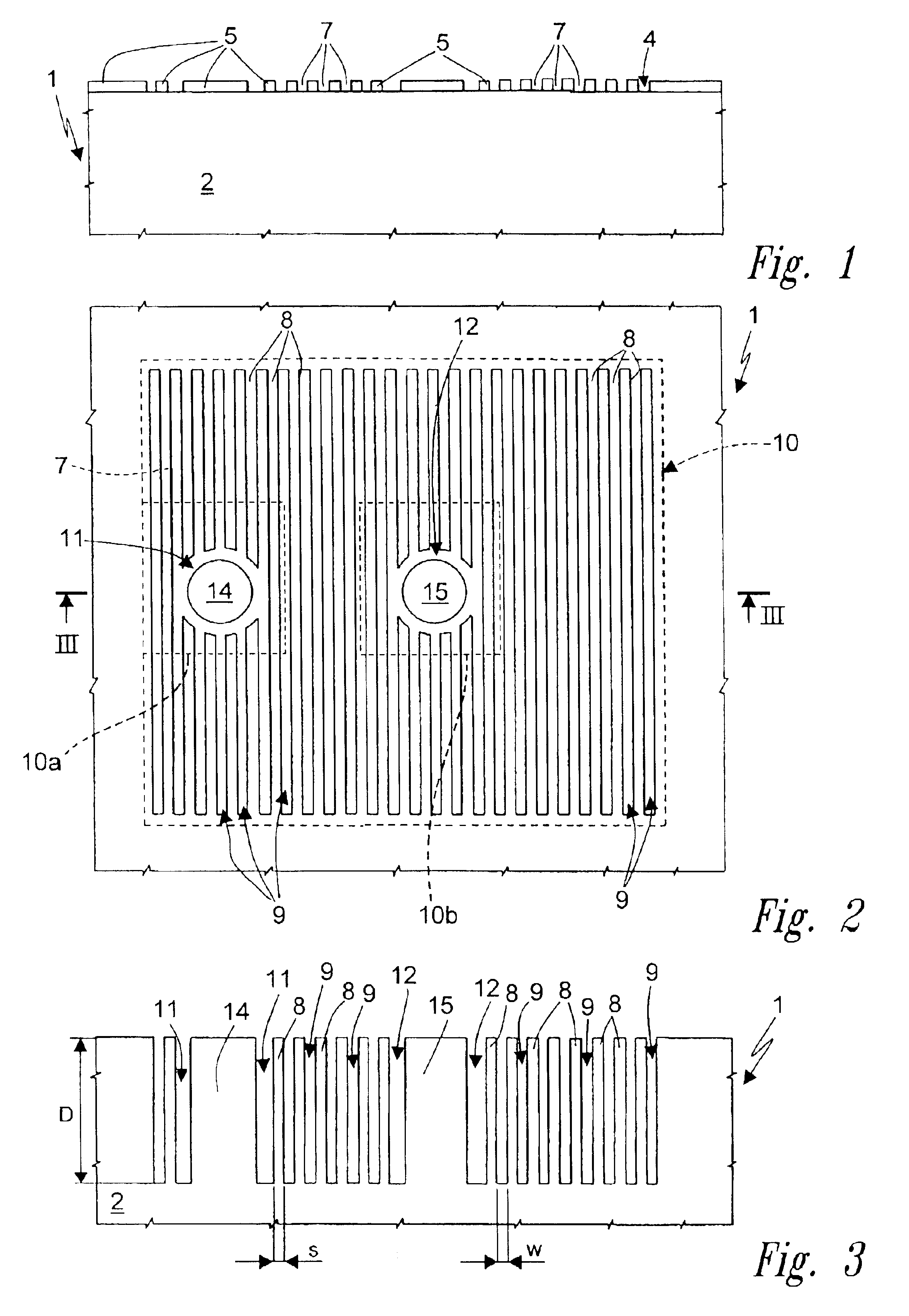
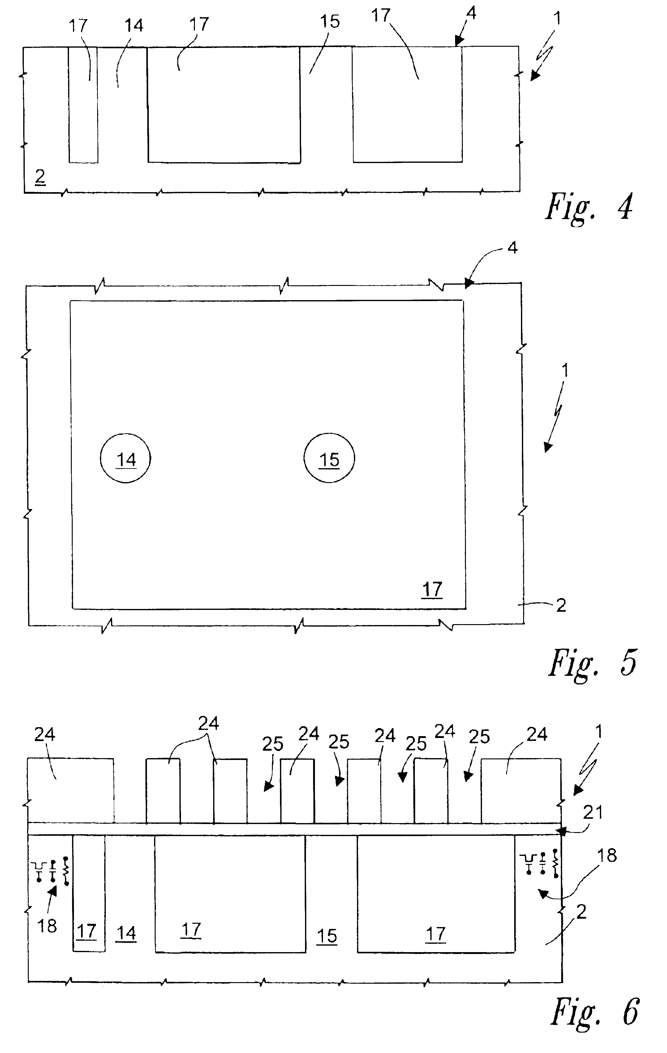
With reference to FIGS. 1-13, a wafer 1 of semiconductor material, such as monocrystalline silicon, comprises a substrate 2 having a doping density of, for example, 1019 atoms / cm3.

Initially, a deep trench etch is performed. For this purpose, an oxide layer is deposited on a first face 4 of the wafer 1 and is then defined by means of a photolithographic process, so as to form a trench mask 5, which leaves partially uncovered a region 7 in which an insulating region will have to be subsequently formed (FIG. 1). Next (FIGS. 2 and 3), the regions 7 of the wafer 1 that have been left uncovered by the trench mask 5 are etched anisotropically a...


PUM


Abstract

A process for manufacturing a semiconductor wafer integrating electronic devices and a structure for electromagnetic decoupling are disclosed. The method includes providing a wafer of semiconductor material having a substrate; forming a plurality of first mutually adjacent trenches, open on a first face of the wafer, which have a depth and a width and define walls); by thermal oxidation, completely oxidizing the walls and filling at least partially the first trenches, so as to form an insulating structure of dielectric material; and removing one portion of the substrate comprised between the insulating structure and a second face of the wafer, opposite to the first face of the wafer.

Description

BACKGROUND OF THE INVENTION1. Field of the InventionThe present invention relates to a process for manufacturing a semiconductor wafer integrating electronic devices and a structure for electromagnetic decoupling.2. Description of the Related ArtAs is known, integration of electronic devices in a single wafer of semiconductor material requires particular solutions in order to decrease the effects of electromagnetic coupling due to the capacitances and mutual parasitic inductances that may form between the regions in which the active and / or passive components and the substrate of the wafer are made. These capacitances and mutual parasitic inductances, in fact, alter the characteristics of the devices and lead to an increase in the overall power dissipation. In addition, the problem of electromagnetic coupling with the substrate is particularly significant in the case of pure passive components, i.e., of those components that are designed to have a behavior of an exclusively capacitiv...

Claims


Application Information

Patent Timeline
IPC IPC(8): H01L21/762H01L21/70H01L21/764H01L27/08
CPCH01L21/76208H01L27/08H01L21/764H01L21/76229
Inventor COMBI, CHANTALFIORITO, MATTEOMOTTURA, MARTAVISALLI, GIUSEPPEVIGNA, BENEDETTO
Owner STMICROELECTRONICS SRL
Why Eureka
Try Eureka