Method and apparatus for determining the temperature of a junction using voltage responses of the junction and a correction factor

a technology of voltage response and temperature measurement, applied in the direction of thermometer testing/calibration, instruments, heat measurement, etc., can solve the problems of inability to obtain the forward voltage vsub>f /sub>, inability to accurately measure the temperature of the junction, and significant computation effort (involving log operations) for each sequence, etc., to achieve accurate and fast measurement of the temperature of the semiconductor junction. , the effect of reducing the computational effor

Inactive Publication Date: 2005-03-22
NAT SEMICON CORP
View PDF4 Cites 43 Cited by
  • Summary
  • Abstract
  • Description
  • Claims
  • Application Information

AI Technical Summary

Benefits of technology

To address the above-discussed deficiencies of the prior art, it is an object of the present invention to provide a method and apparatus for measuring the temperature of a semiconductor junction based on a pre-calculated correction factor. Other objects of the present invention are to provide a method and apparatus that (i) substantially reduces the computational effort involved in a temperature measurement of a semiconductor junction, (ii) measures the temperature of a semiconductor junction that is based on a p

Problems solved by technology

However, due to parasitic effects (e.g., contact resistance), a precise measurement of the junction forward voltage Vf can not be obtained.
The Ohmic resistances rc, rb, and re, illustrated in FIG. 1, are the main obstacle in obtaining an accurate measurement of the forward voltage Vf of the junction.
While this method improves the resu

Method used


Image

  • Method and apparatus for determining the temperature of a junction using voltage responses of the junction and a correction factor
  • Method and apparatus for determining the temperature of a junction using voltage responses of the junction and a correction factor
  • Method and apparatus for determining the temperature of a junction using voltage responses of the junction and a correction factor

Examples


Embodiment Construction

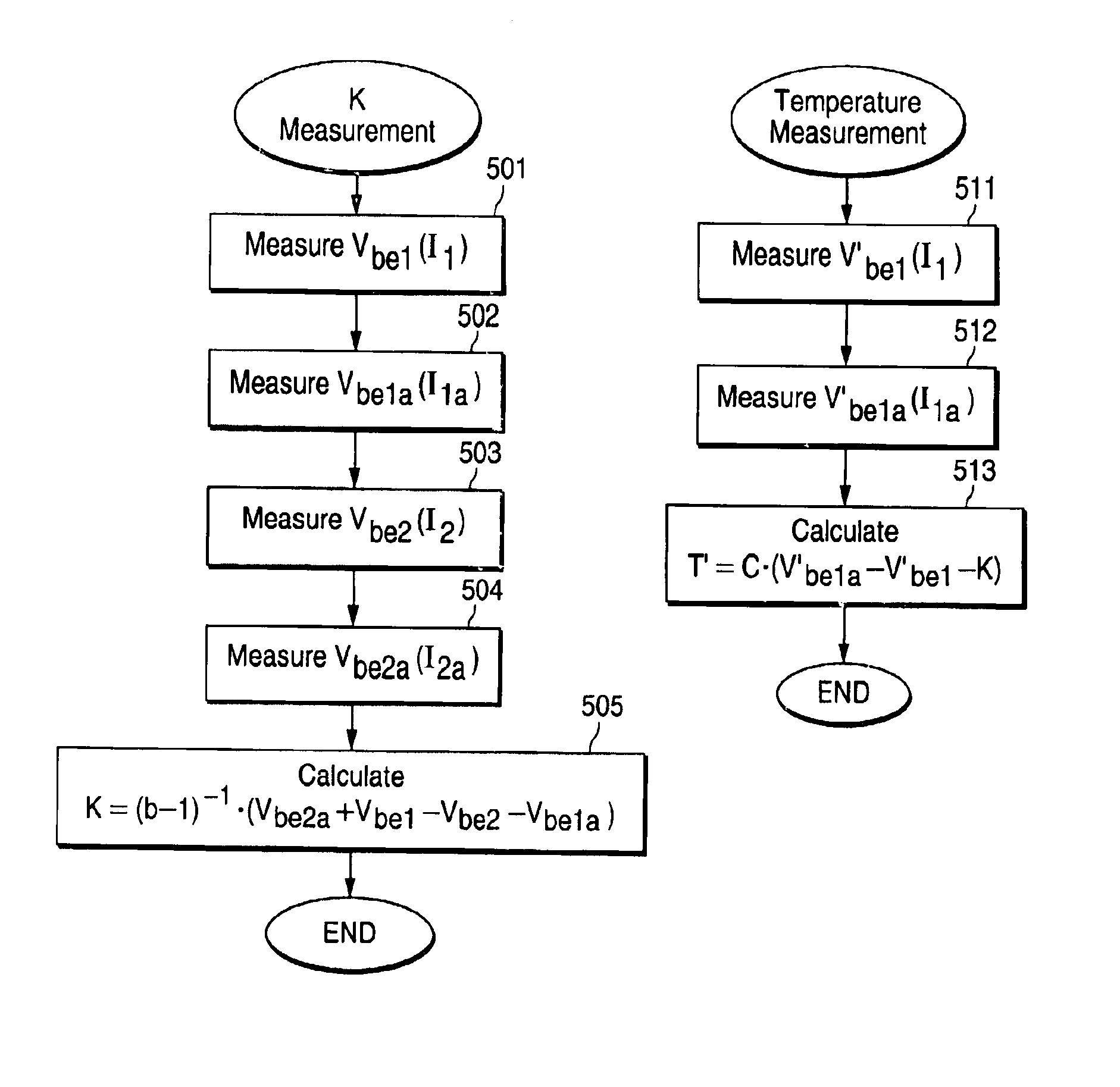
The present invention provides a fast and accurate method for obtaining temperature measurement of a semiconductor junction. According to a preferred embodiment of the invention, a correction factor is calculated to enable an accurate computation of the junction temperature. The computation of the correction factor involves four voltage measurements, and the temperature measurement performed thereafter requires only two voltage measurements of the junction. Thus, with this method junction temperature is obtained by utilizing less voltage measurements, and less computation efforts, per measurement, in comparison with prior art methods. As will be explained in details hereinafter, these advantages can be further exploited to develop simplified temperature measurement devices.

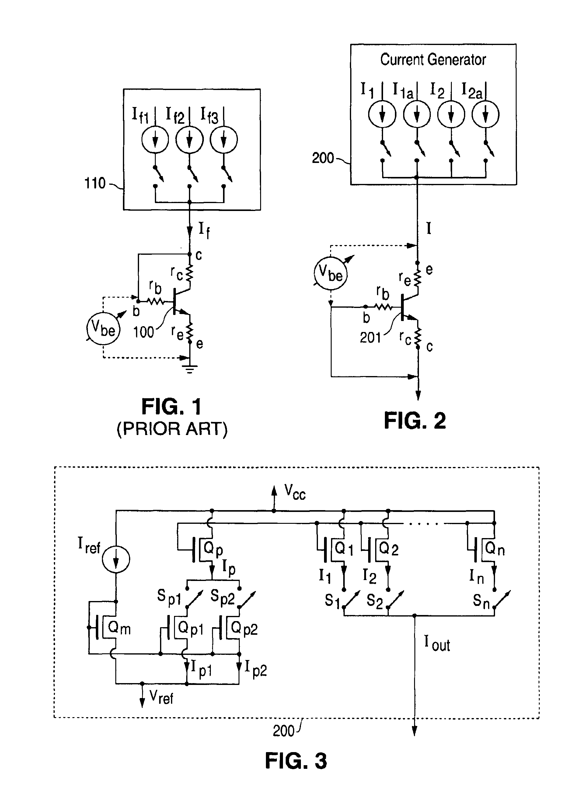
FIG. 2 illustrates a measurement array, in which current generator 200 is used to generate forward currents of four different magnitudes I=I1, I1a, I2, or I2a. The currents magnitudes produced by the current gener...


PUM


Abstract

Method and system for periodically measuring the junction temperature of a semiconductor device. The junction exited by at least two sequential predetermined currents of different magnitudes the voltage response of the junction to the at least two currents is measured and the temperature of the junction is calculated, while substantially canceling ohmic effects, by using the voltage response and a correction factor obtained by periodically. Whenever desired, the junction is exited by a set of at least four sequential different currents having known ratios. The voltage response to the set is measured and the correction factor is calculated by using each voltage response to the set.

Description

TECHNICAL FIELD OF THE INVENTIONThe present invention relates generally to the field of temperature measurement in semiconductor circuitry, and, more particularly, to a method and apparatus for determining the temperature of a semiconductor junction utilizing a correction factor to eliminate the effects of parasitic Ohmic resistances.BACKGROUND OF THE INVENTIONIn many applications there is a need to keep an operating system within predefined temperature ranges. A common type of temperature sensing device used for this task is known as a “contact device,” which is relatively inexpensive and can be used to accurately measure temperature. A contact device operates in direct contact with a measured object. In this way, the contact device senses the temperature of the object thereby generating a temperature measurement can be obtained.One type of contact device temperature sensor is based on a semiconductor junction (usually Silicon or Germanium), which can be compactly packaged as a sma...

Claims


Application Information

Patent Timeline
IPC IPC(8): G01K7/01G01K15/00
CPCG01K15/00G01K7/01
Inventor FALIK, OHAD
Owner NAT SEMICON CORP
Why Eureka
Try Eureka