Liquid crystal display device having a black matrix with a specific resistance

Inactive Publication Date: 2005-03-22
GOLD CHARM LTD
View PDF15 Cites 8 Cited by
  • Summary
  • Abstract
  • Description
  • Claims
  • Application Information

AI Technical Summary

Benefits of technology

According to the present invention, because the color layers are formed so as to be spaced apart from at least the gate lines, the color layers are unsusceptible to a change in voltage at least on the gate lines. Hence, when a voltage is applied to the gate lines, no charges are injected into the color layers by the applied voltage. For this reason, there will be developed no vertical electric field across the color layers and pixel electrodes such that disturbs the orientation of the liquid crystal molecules. In addition, in case that the color layers are formed apart from the drain lines also, the color layers are also unsusceptible to a change in voltage on the drain lines, and therefore, the orientation becomes more resistant to disturbance.
In addition, because no color layers are formed above the gate lines, an equivalent circuit in a space between the gate lines and pixel elect

Problems solved by technology

Consequently, a charge distribution within the color filter is changed by an electric field applied to the liquid crystal, and an electric field is developed in the vertical direction, which disturbs the electric field in the lateral direction.
S

Method used


Image

  • Liquid crystal display device having a black matrix with a specific resistance
  • Liquid crystal display device having a black matrix with a specific resistance
  • Liquid crystal display device having a black matrix with a specific resistance

Examples


first embodiment

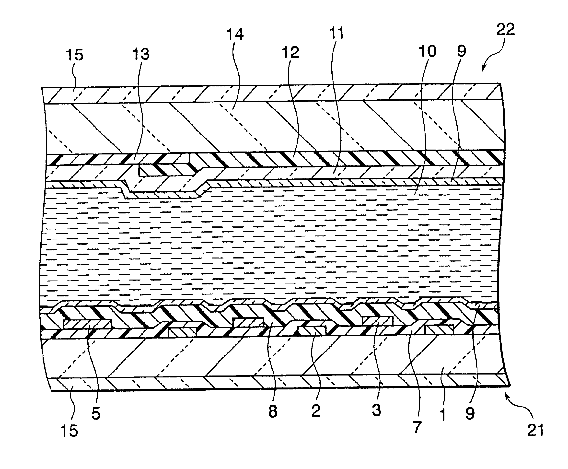
In the first place, a manufacturing method of an IPS mode liquid crystal display in accordance with the first embodiment will be explained.

After a metal layer, which will be made into gate lines 6, common electrodes 2, and common electrode lines 2a, is deposited over a transparent substrate 1 for a TFT substrate 21, the metal layer is patterned into a predetermined shape. Then, a gate insulation film 7 is deposited on the metal layer, and an amorphous silicon film and an n+ amorphous silicon film are deposited in succession. Then, the amorphous silicon film and n+ amorphous silicon film are patterned into an island shape, thereby forming a TFT 4 region. Then, a contact region (not shown), in which a metal layer connected to the gate line 6 and common electrode line 2a is buried, is formed in a predetermined region in the gate insulation film 7. Then, a metal layer, which will be made into the drain line 5 and pixel electrode 3, is deposited and patterned into a predetermined shape. ...


PUM


Abstract

A first substrate, a second substrate opposing to the first substrate, and liquid crystal provided in a space between the first substrate and second substrate are provided to an IPS mode liquid crystal display. A plurality of gate lines and a plurality of drain lines, thin film transistors, pixel electrodes, and common electrodes are formed on a transparent substrate in a first substrate. Each of the thin film transistors is provided in a vicinity of the intersection of the gate line and drain line. Each of the pixel electrodes is formed within a pixel region enclosed with an adjacent pair of the gate lines and an adjacent pair of the drain lines. Each of the common electrodes develops an electric field within each of the pixel regions between the pixel electrode and itself. The second substrate includes color layers provided for each of the pixel regions. The color layers are spaced apart from the gate lines and drain lines when seen on a plane.

Description

BACKGROUND OF THE INVENTION1. Field of the InventionThe present invention relates to an IPS (In-Plane Switching) mode liquid crystal display which rotates liquid crystal in a plane substantially parallel to a TFT substrate by applying a voltage across a pixel electrode and a common electrode formed in the TFT substrate, and more particularly to a liquid crystal display achieving enhanced contrast.2. Description of the Related ArtIn an active matrix type liquid crystal display, for example, thin film transistors (TFTs) are employed as pixel switching elements. Also, the active matrix type liquid crystal display attains a satisfactory image quality. For this reason, the active matrix type liquid crystal display is employed extensively as a monitor of a space-saving type desktop computer or the like. Generally, a liquid crystal display includes two operating modes: the twisted nematic (TN) mode, by which directors of aligned liquid crystal molecules are rotated in a direction perpendic...

Claims


Application Information

Patent Timeline
IPC IPC(8): G02F1/1335G02F1/13G02F1/1343G02F1/1345G02F1/133G02F1/136G02F1/1368G09F9/30G09G3/20G09G3/36
CPCG02F1/133514G02F1/133512G02F1/1345G02F1/134363G02F1/1343
Inventor SHIBAHARA, HIDEOMATSUMOTO, KIMIKAZU
Owner GOLD CHARM LTD
Why Eureka
Try Eureka