Semiconductor material and method for enhancing solubility of a dopant therein

Inactive Publication Date: 2005-03-29
LAWRENCE LIVERMORE NAT SECURITY LLC
View PDF8 Cites 0 Cited by
  • Summary
  • Abstract
  • Description
  • Claims
  • Application Information

AI Technical Summary

Benefits of technology

It is an object of the present invention to increase the s

Problems solved by technology

However, an undesirable effect of ion-implantation is that it introduces significant damage into the silicon wafer in the form of point defects and their clusters, Fahey et al Rev. Mod. Phys. 61, 289 (1989).
The annealing procedure leads to unwanted dopant diffusion, as well as nucleation and growth of dopan

Method used


Image

  • Semiconductor material and method for enhancing solubility of a dopant therein
  • Semiconductor material and method for enhancing solubility of a dopant therein
  • Semiconductor material and method for enhancing solubility of a dopant therein

Examples


Embodiment Construction

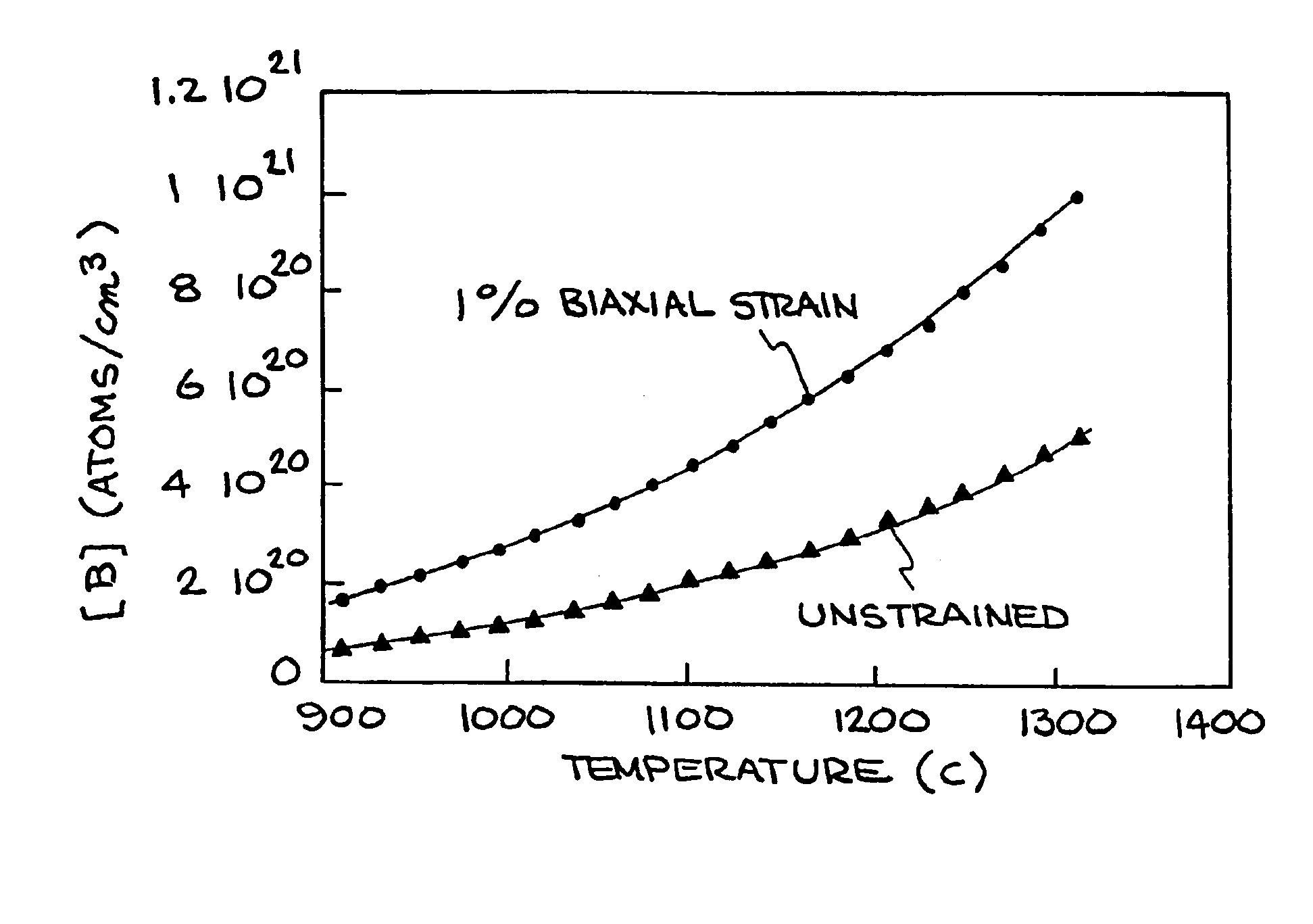
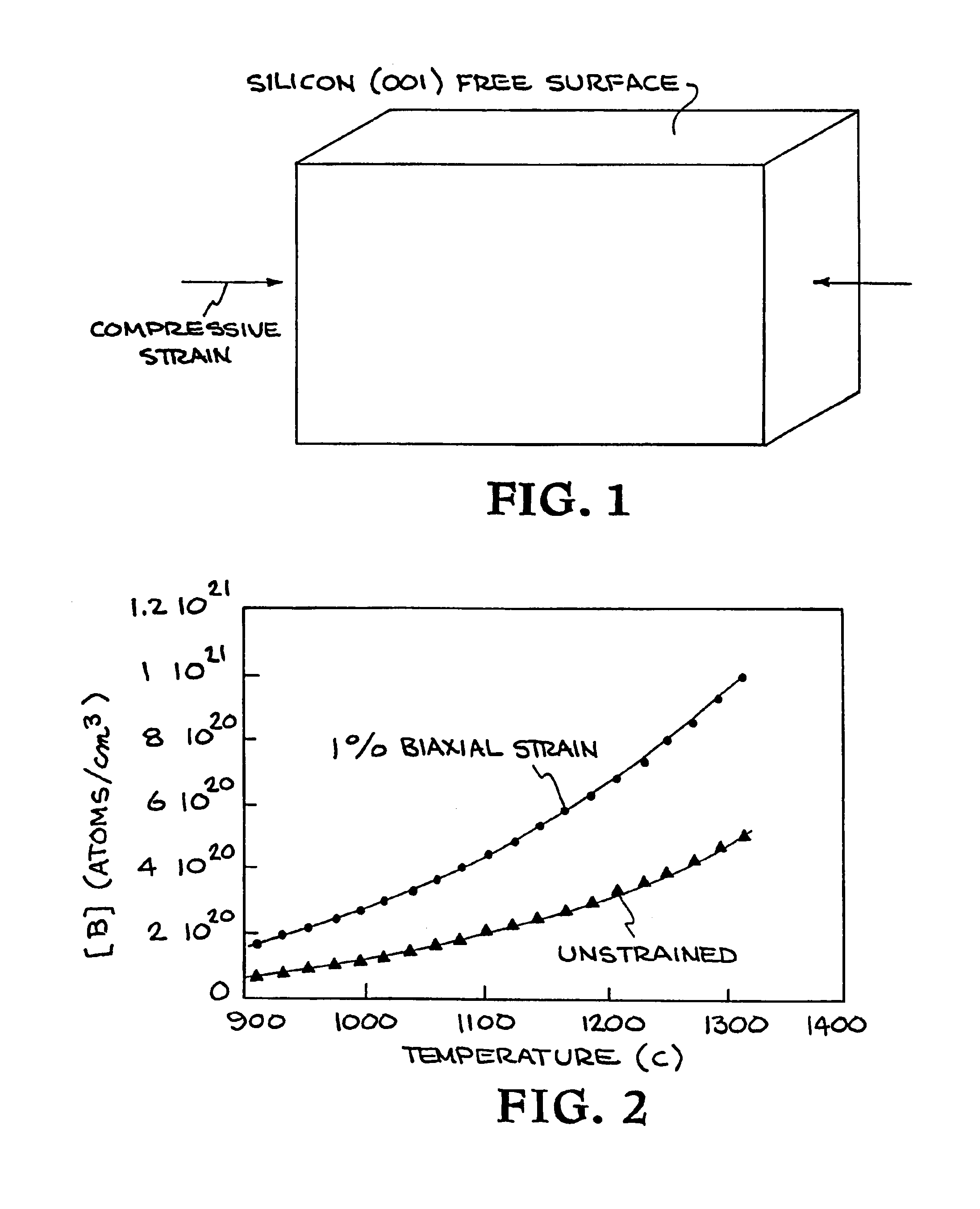
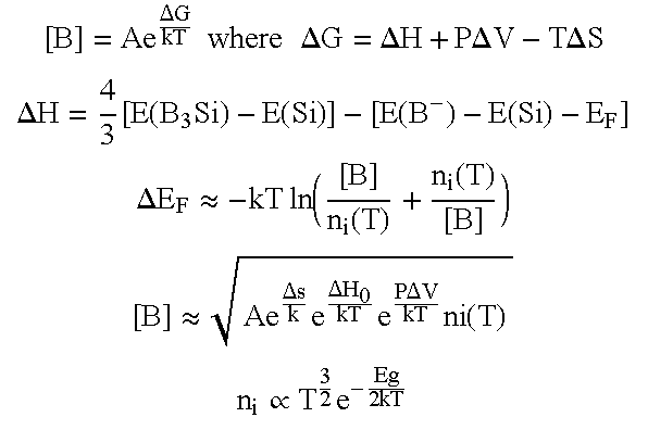
The present invention involves increasing the solubility of dopants in semiconductor materials, particularly increasing the solubility of boron and indium in silicon. This is basically accomplished by placing a strain on the silicon at elevated temperatures. For example, it has been demonstrated that a 1% compressive strain raises the equilibrium solubility by 100% at 1100° C. for boron, and for indium a 1% tensile strain at 1100° C. corresponds to an enhancement of solubility by 200%. This method for enhancing the solubility of boron and indium in silicon resulted from the performance of first-principles quantum mechanical calculation relative to the temperature dependence of the equilibrium solubility of two important p-type dopants in silicon, namely boron and indium under various strain conditions. It was found that the equilibrium thermodynamic solubility of size-mismatched impurities, such as boron and indium in silicon, can be raised significantly if the silicon substrate is ...


PUM


Abstract

A method for enhancing the equilibrium solubility of boron ad indium in silicon. The method involves first-principles quantum mechanical calculations to determine the temperature dependence of the equilibrium solubility of two important p-type dopants in silicon, namely boron and indium, under various strain conditions. The equilibrium thermodynamic solubility of size-mismatched impurities, such as boron and indium in silicon, can be raised significantly if the silicon substrate is strained appropriately. For example, for boron, a 1% compressive strain raises the equilibrium solubility by 100% at 1100° C.; and for indium, a 1% tensile strain at 1100° C., corresponds to an enhancement of the solubility by 200%.

Description

BACKGROUND OF THE INVENTIONThe present invention relates to solubility of dopants in semiconductor materials, particularly to enhancing the solubility, and more particularly to a method for enhancing solubility of boron and indium in silicon.Ion implantation allows for exceptional control and reproducibility in the introduction of dopants into the near-surface region of semiconductors. As a result, it has been the universal method of choice for doping MOS transistors in silicon-based integrated circuits since the beginning of the semiconductor revolution. However, an undesirable effect of ion-implantation is that it introduces significant damage into the silicon wafer in the form of point defects and their clusters, Fahey et al Rev. Mod. Phys. 61, 289 (1989). For a device to be operational these defects must be removed and the dopants electrically activated through high-temperature annealing. The annealing procedure leads to unwanted dopant diffusion, as well as nucleation and growt...

Claims


Application Information

Patent Timeline
IPC IPC(8): C30B33/00H01L29/02H01L29/161H01L29/10
CPCC30B33/00H01L29/161H01L29/7842C30B29/605H01L29/1054
Inventor SADIGH, BABAKLENOSKY, THOMAS J.DIAZ DE LA RUBIA, TOMASGILES, MARTINCATURLA, MARIA-JOSEOZOLINS, VIDVUDSASTA, MARKTHEISS, SILVAFOAD, MAJEEDQUONG, ANDREW
Owner LAWRENCE LIVERMORE NAT SECURITY LLC
Why Eureka
Try Eureka