Method for preventing polysilicon mushrooming during selective epitaxial processing

a polysilicon and epitaxial processing technology, applied in the field of semiconductor devices, can solve the problems of reducing the channel length of the transistor, degrading performance, scaling the mos transistor, and affecting the performance of the transistor,

a polysilicon and epitaxial processing technology, applied in the field of semiconductor devices, can solve the problems of reducing the channel length of the transistor, degrading performance, scaling the mos transistor, and affecting the performance of the transistor,

US6872610B1Active Publication Date: 2005-03-29TEXAS INSTR INC

Image

  • Method for preventing polysilicon mushrooming during selective epitaxial processing
  • Method for preventing polysilicon mushrooming during selective epitaxial processing
  • Method for preventing polysilicon mushrooming during selective epitaxial processing

Examples


Embodiment Construction

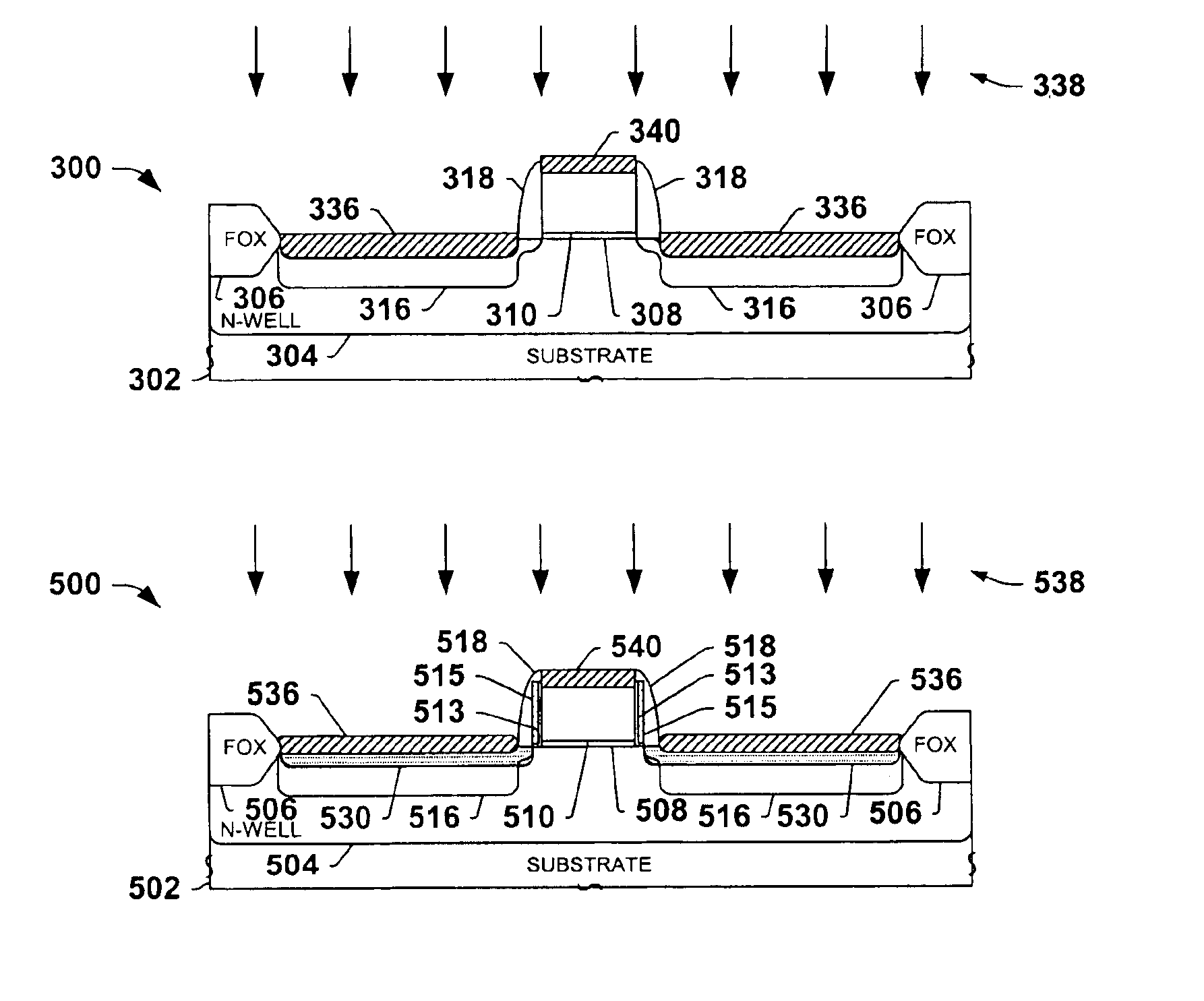
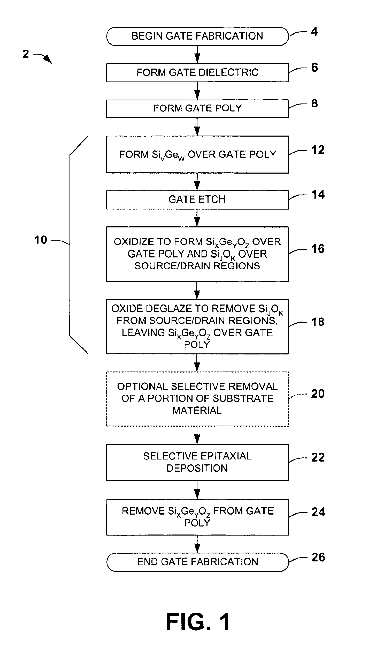
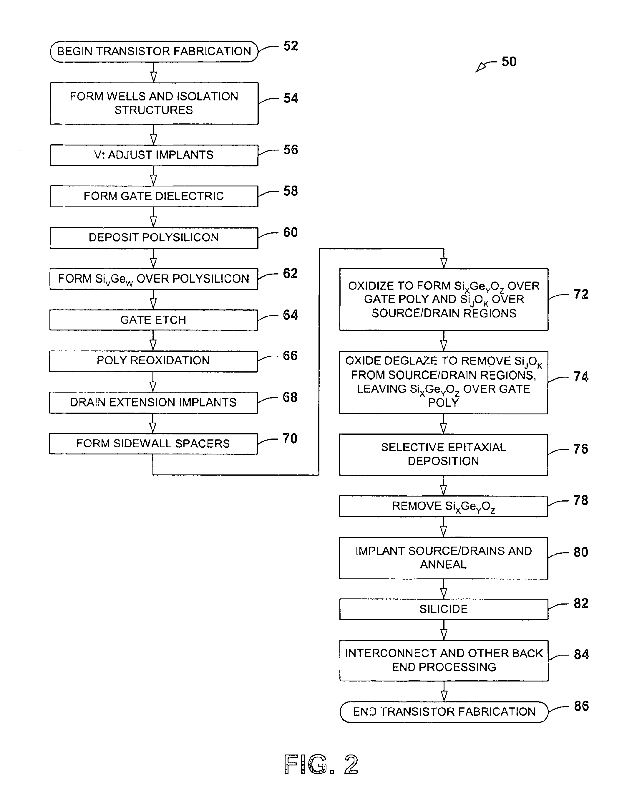
One or more implementations of the present invention will now be described with reference to the attached drawings, wherein like reference numerals are used to refer to like elements throughout. The invention relates to semiconductor devices formed using selective epitaxial deposition or growth processes, wherein poly mushrooming is prevented or inhibited by providing a protection layer above a patterned gate structure during the selective deposition. The invention is illustrated and described below in conjunction with exemplary PMOS transistors in which deposited silicon is used in forming elevated or raised source / drains or to fill in recesses in recessed source / drain or recessed HDD transistors. However, the invention may be employed, alternatively or in combination, in fabricating NMOS transistors, wherein the invention is not limited to the illustrated examples, and wherein the illustrated structures are not necessarily drawn to scale.

Referring initially to FIG. 1, an exemplary...


PUM


Abstract

Methods are presented, in which an oxide protection layer is provided on a gate structure for protection against poly mushrooming during selective epitaxial silicon deposition in fabricating elevated or recessed source transistors. In one implementation, the protection layer is constructed by depositing silicon germanium over a gate polysilicon layer prior to gate patterning, and oxidizing the device to form a silicon germanium oxide over the gate polysilicon. The protection layer is then removed following selective epitaxial deposition.

Description

FIELD OF INVENTIONThe present invention relates generally to semiconductor devices and more particularly to methods for fabricating transistors while avoiding polysilicon mushrooming during selective epitaxial deposition processes.BACKGROUND OF THE INVENTIONField effect transistors (FETs) are widely used in the electronics industry for switching, amplification, filtering, and other tasks related to both analog and digital electrical signals. Most common among these are metal-oxide-semiconductor field-effect transistors (MOSFETs), wherein a gate contact or electrode is energized to create an electric field in a channel region of a semiconductor body, by which electrons are allowed to travel through the channel between a source region and a drain region of the semiconductor body. The source and drain regions are typically formed by adding dopants to targeted regions on either side of the channel. A gate dielectric or gate oxide is formed over the channel, and a gate electrode or gate ...

Claims


Application Information

Patent Timeline
29 Mar 2005
Publication
US6872610B1
IPC
H01L21/02; H01L21/336; H01L21/20; H01L29/78
CPC
H01L29/66545; H01L29/66628; H01L29/66636; H01L29/665; H01L21/02381; H01L21/02532; H01L21/02639; H01L21/02664
Inventors
MANSOORI, MAJID M.; WU, ZHIGIANG