

Trench capacitors with reduced polysilicon stress
- Summary
- Abstract
- Description
- Claims
- Application Information
AI Technical Summary
Benefits of technology
Problems solved by technology
Method used
Image

Examples
second embodiment
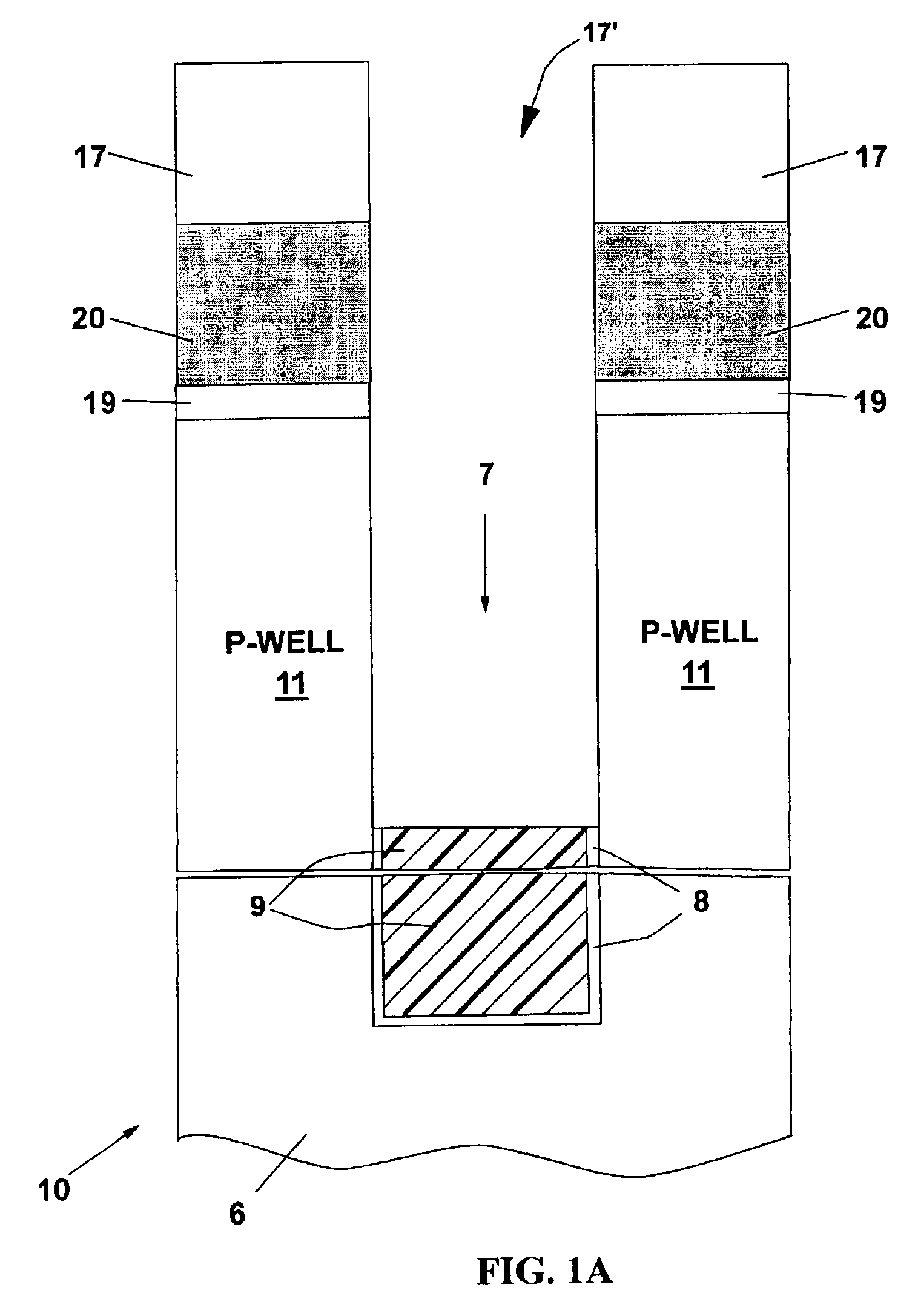
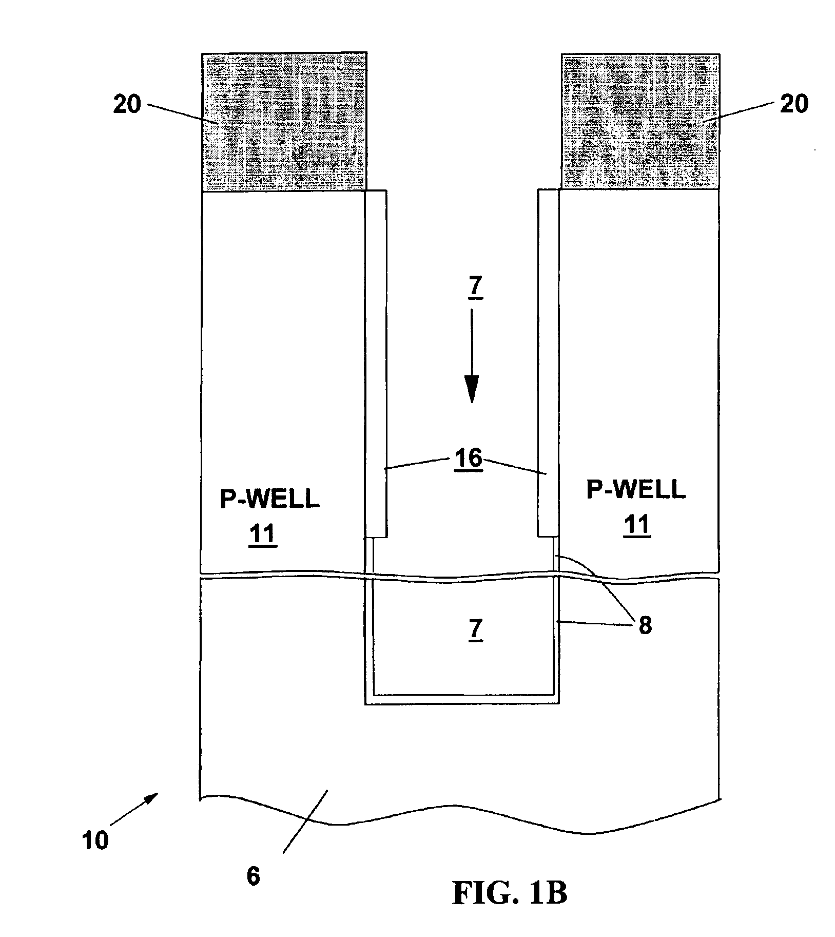
FIGS. 2A-2E illustrate the process steps for forming a second embodiment of a deep trench capacitor 110 manufactured in accordance with a second processing sequence in accordance with this invention, which is a modification of the process of FIGS. 1A-1J.
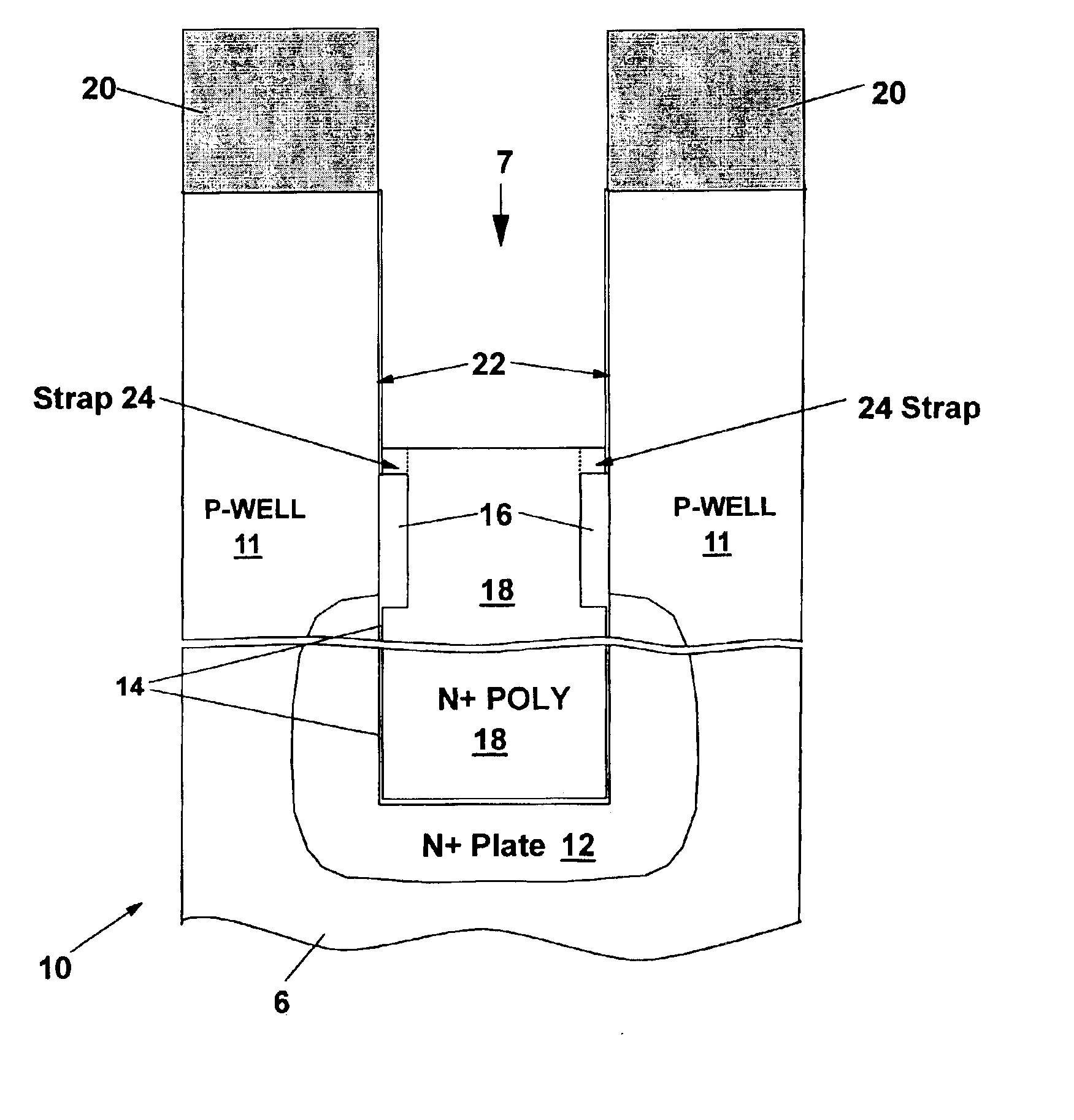
FIG. 2A is similar to FIG. 1F with like reference numbers identifying like elements in the drawings. The capacitor 110 is formed in the substrate 106 of a microcircuit device and the deep trench 107 has the N+ doped electrode comprising the outer capacitor plate electrode 12 formed at the bottom of the substrate 106. The node dielectric layer 14 is formed on the surface of the inner, storage node electrode 12. The isolation collar 16 is formed on the walls of the deep trench 107 bridging from the inner, storage node electrode 18 up along the sidewalls of the P-well 11.
As in FIG. 1F, the isolation collar 16 of FIG. 2A has been etched back until it is substantially recessed below the top of the inner, storage node electrode 18 and ther...
PUM
 Abstract
Description
Claims
Application Information