Method of fabricating nonvolatile semiconductor memory device

a nonvolatile, memory device technology, applied in the direction of semiconductor devices, basic electric elements, electrical appliances, etc., can solve the problems of difficult to form miniaturized cmos circuits with high performance and nonvolatile semiconductor memory devices on the same substrate, adversely affecting various impurity concentrations, etc., to suppress damage to tunnel insulation films and eliminate long heat treatment period

Inactive Publication Date: 2005-03-29
PANASONIC CORP
View PDF18 Cites 7 Cited by
  • Summary
  • Abstract
  • Description
  • Claims
  • Application Information

AI Technical Summary

Benefits of technology

In view of the above described conventional problems, an objective of the present invention is to eliminate a long period of heat treatment required for the impurity diffusion process while suppressing damage to tunnel insulation films caused by injection of impurity ions when forming the source diffusion layer and the drain diffusion layer, which are located at side portions of the gate structure.

Problems solved by technology

If, a MOS type semiconductor device that controls a nonvolatile semiconductor memory device or a micro controller that requires high speed operation or a MOS type semiconductor device for micro processor, is formed on the same substance, this extended period of time of heat treatment adversely affects various impurity concentrations such as channel impurity of a MOS type transistor.
Therefore, because the recent CMOS technology, which requires high performance and miniaturization, tries to reduce thermal hysteresis to as small as possible, if this trend continues, a problem is generated that it would be difficult to form miniaturized CMOS circuits with high performance and nonvolatile semiconductor memory devices on the same substrate.
This generates a problem that the insulation film 102 cannot be miniaturized.
In this case, also, it is difficult to miniaturize the insulation film 102.
Furthermore, in the conventional fabrication method, if the film thickness of the insulative side wall spacer 111 is reduced too much, a problem is generated that injected arsenic ions cause damage to the thermal oxidation silicon film 110 formed on the side surfaces of the gate structure 107 and located beside the gate structure 107.

Method used


Image

  • Method of fabricating nonvolatile semiconductor memory device
  • Method of fabricating nonvolatile semiconductor memory device
  • Method of fabricating nonvolatile semiconductor memory device

Examples


embodiment 1

A Variation of Embodiment 1

Variation of Embodiment 1 of the present invention is explained in the following by referring to figures.

FIG. 3A to FIG. 3C are cross sectional views which show a process sequence for a method of fabricating a nonvolatile semiconductor memory device in a variation of Embodiment 1 of the present invention. In FIG. 3A to FIG. 3C, components that are the same as the components of FIG. 1A to FIG. 1C are denoted by the same reference numbers and symbols.

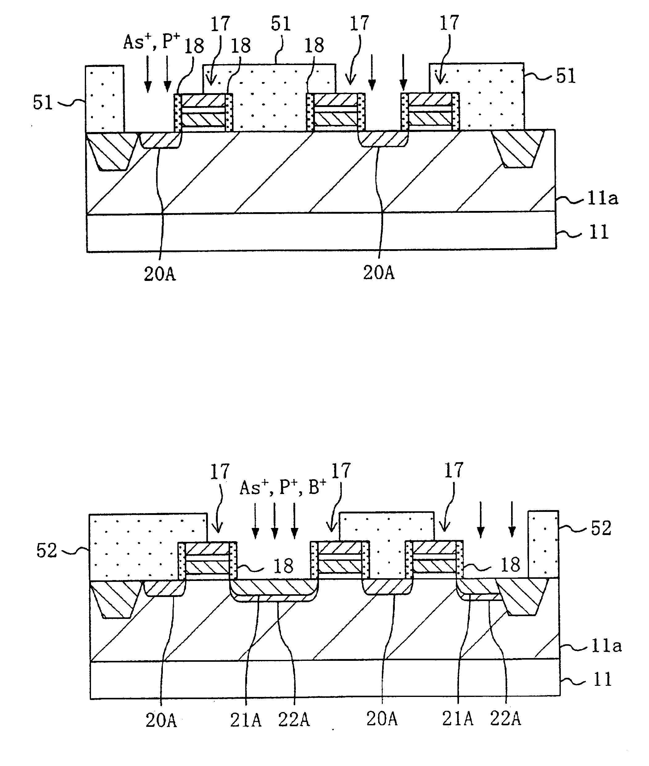
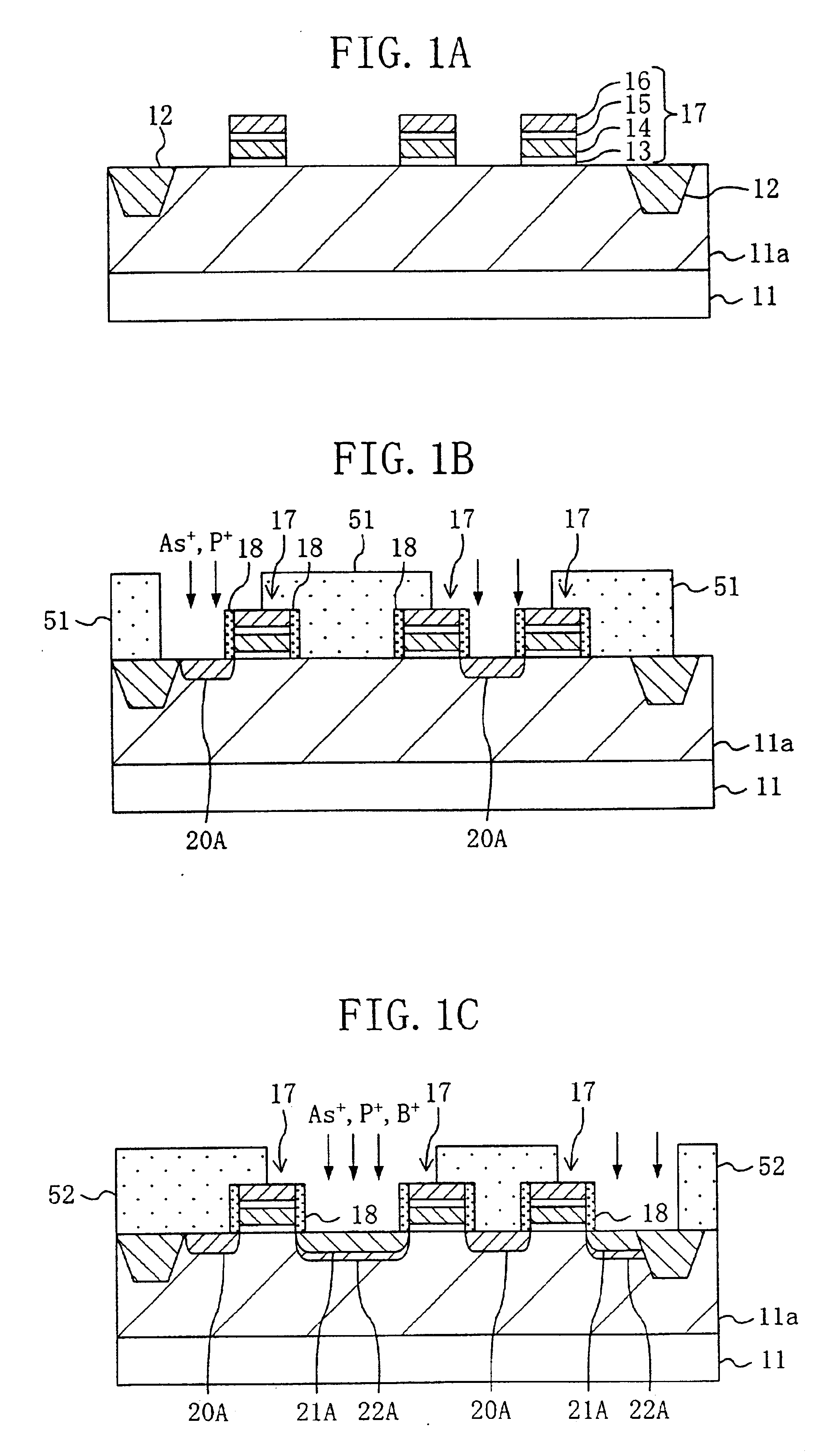
First, as shown in FIG. 3A, a p-type well 11A and an insulation film 12, in this order, are formed above a semiconductor substrate 11. Then, a film 13A for forming a tunnel insulation film composed of silicon oxide, a film 14A for forming a floating gate electrode of poly-silicon, a film 15A for forming a capacitor insulator film composed of silicon oxide or silicon nitride, and a film 16A for forming a control gate electrode of poly-silicon having about 70 nm film thickness are sequentially deposited on the ent...

embodiment 2

Variation of Embodiment 2 of the present invention is explained in the following by referring to figures.

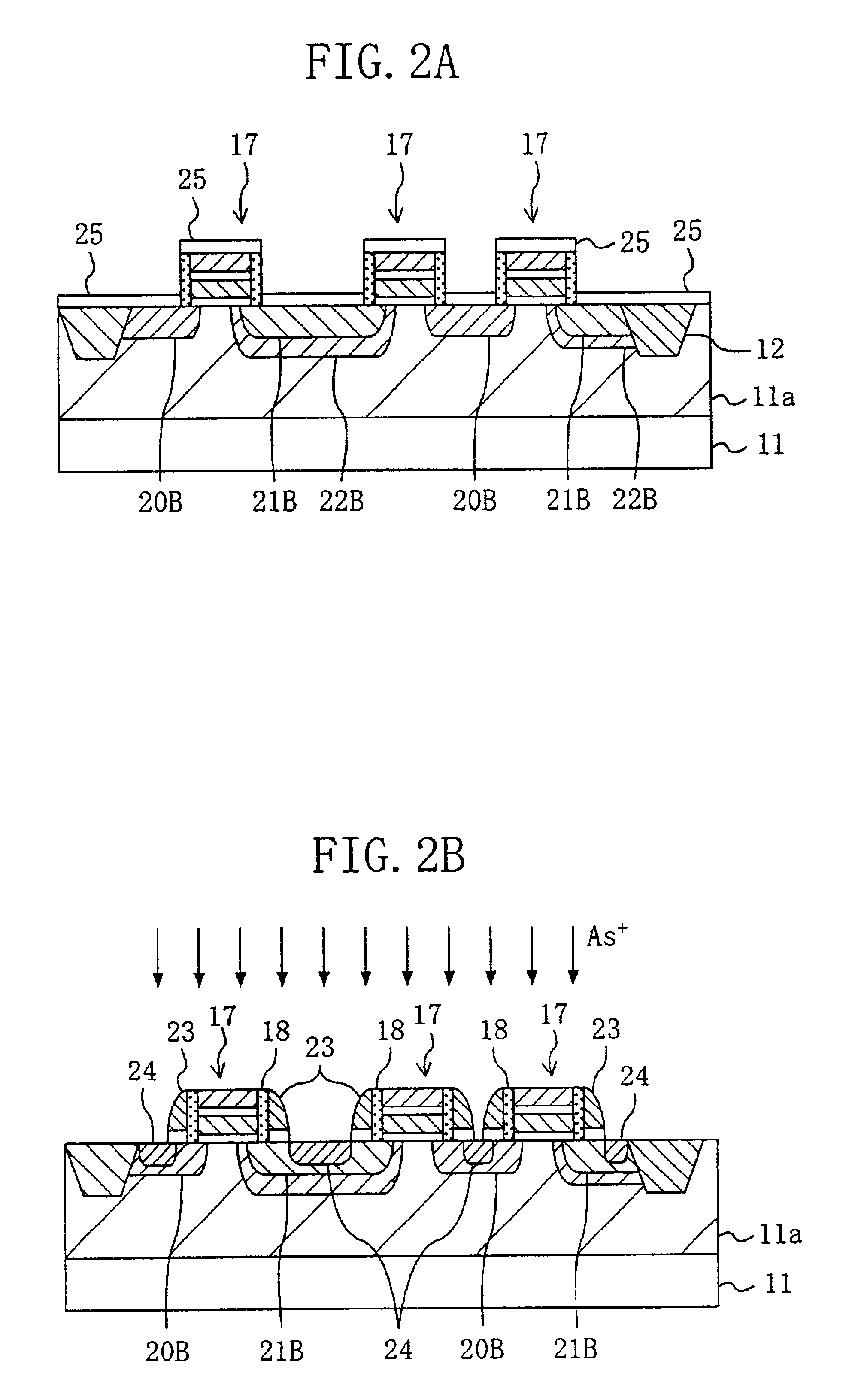
FIG. 6A to FIG. 6C are cross sectional views which show a process sequence for the method of fabricating a nonvolatile semiconductor memory device in a variation of Embodiment 2 of the present invention. Here, one gate structure and ion injection adjustment film are used to explain general fabrication methods. Also, in FIG. 6A to FIG. 6C, components which are the same as the components of FIG. 4A to FIG. 4C are denoted by the same reference numerals and symbols.

A feature of this variation example is that the ion injection adjustment film is made by a multi-layer structure of silicon oxide and silicon nitride that are formed sequentially from the gate structure side.

First, as shown in FIG. 6A, a p-type well 11a is formed on a semiconductor substrate 11 composed of p-type silicon, and, then, a gate structure 17 composed of a tunnel insulation film 13, a floating gate electrode 14, ...


PUM


Abstract

A gate structure composed of a tunnel insulation film, a floating gate electrode, a capacitive insulation film and a control gate electrode is formed on a semiconductor substrate. Then, ion injection adjustment films that are in contact with the floating gate electrode at least on the side surfaces of the floating gate electrode are formed. After injecting impurity ions into the active region beside the gate structure in the semiconductor substrate while using the gate structure and the ion injection adjustment film as masks, the injected impurity ions are diffused thermally by performing heat treatment on the active region. Film thickness of the ion injection adjustment film is selected to a value to prevent the impurity ions from being injected into the tunnel insulation film and allows the impurity ions to reach lower portions of side end of the floating gate electrode in the active region as a result of diffusive scattering of impurity ions in the semiconductor substrate.

Description

BACKGROUND OF THE INVENTIONThe present invention relates to a method of fabricating a nonvolatile semiconductor memory device, and particularly relates to a method of fabricating an electrically erasable nonvolatile semiconductor memory device such as a large capacity EPROM device, EEPROM device and flash memory device.Conventional fabrication methods of nonvolatile semiconductor memory devices are described in Japanese Patent Laid-Open Publication No. Hei 5-251712 (referred to as the first conventional example hereafter) or Japanese Patent Publication No. 2515715 (referred to as the second conventional example hereafter).Conventional fabrication methods of nonvolatile semiconductor memory devices are explained below by referring to the figures.FIG. 7A to FIG. 7C and FIG. 8 are cross sectional views which show a process sequence for conventional fabrication methods of nonvolatile semiconductor memory devices.First, as shown in FIG. 7A, a p-type well 101a is formed on a semiconductor...

Claims


Application Information

Patent Timeline
Patent Type & Authority Patents(United States)
IPC IPC(8): H01L21/70H01L27/115H01L21/28H01L29/423H01L21/02H01L21/8247H01L29/40
CPCH01L21/28273H01L29/42324H01L27/11521H01L27/115H01L29/40114H10B69/00H10B41/30
Inventor ODAKE, YOSHINORINORO, FUMIHIKOHASHIDZUME, TAKAHIKO
Owner PANASONIC CORP
Why Eureka
Try Eureka