Methods of positioning and/or orienting nanostructures

a technology of nanostructures and nanowires, applied in the field of nanotubes, nanocrystals, nanowires, can solve the problems of insufficient availability of commercially viable products, inaccurate and reproducible positioning of these materials,

Inactive Publication Date: 2005-03-29
ONED MATERIAL INC
View PDF39 Cites 426 Cited by
  • Summary
  • Abstract
  • Description
  • Claims
  • Application Information

AI Technical Summary

Benefits of technology

In a further aspect, the invention is directed to methods of positioning nanowires in one or more predetermined regions on a substrate. The methods typically comprise providing a substrate having a first surface, overlaying the first surface with a mask, where the mask provides fluid access to one or more first predetermined regions on the first surface, but not to one or more second predetermined regions on the surface of the substrate. A fluid containing nanowires is then flowed through the mask and into contact with the first predetermined regions of the substrate surface. The nanowires contained in the nanowire containing fluid are then permitted to immobilize in the first predetermined regions of the surface of the substrate.
In another aspect, the invention is directed to one or more populations of nanowires immobilized on a planar surface of a substrate, where the population(s) of nanowires are substantially longitudinally oriented in a first direction parallel to the planar surface.

Problems solved by technology

While commercial applications of the molecular, physical, chemical and optical properties of these materials have been postulated for all of these different types of materials, generating commercially viable products has not, as yet, been forthcoming.
In the world of devices with integrated nanomaterial elements, some of the difficulties in producing commercially viable products has stemmed from the difficulty in handling and interfacing with such small scale materials.
Accurate and reproducible positioning of these materials has proven difficult.

Method used


Image

  • Methods of positioning and/or orienting nanostructures
  • Methods of positioning and/or orienting nanostructures
  • Methods of positioning and/or orienting nanostructures

Examples


example 1

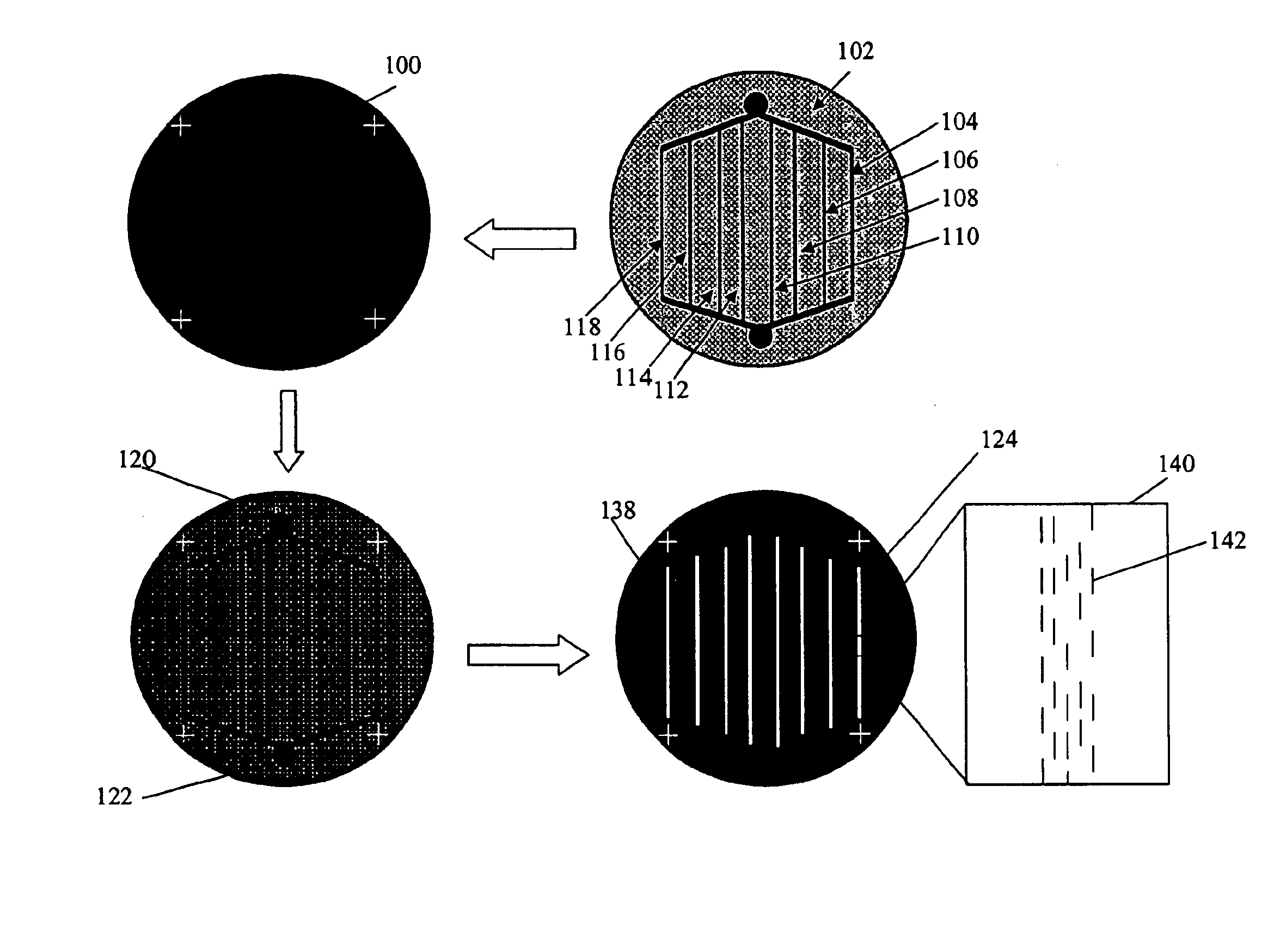
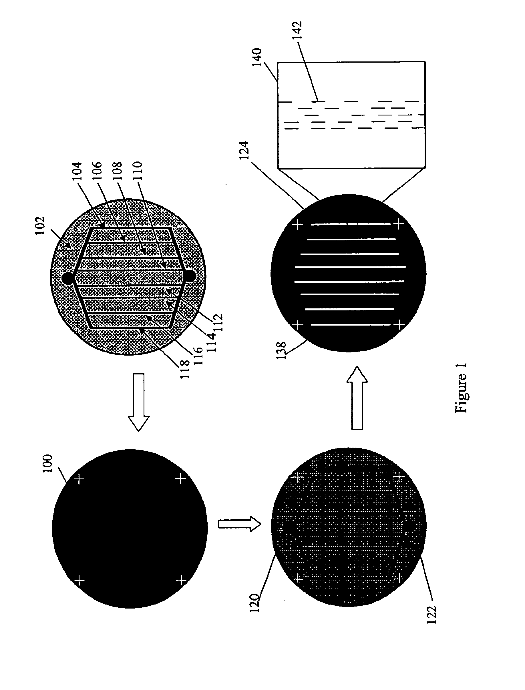
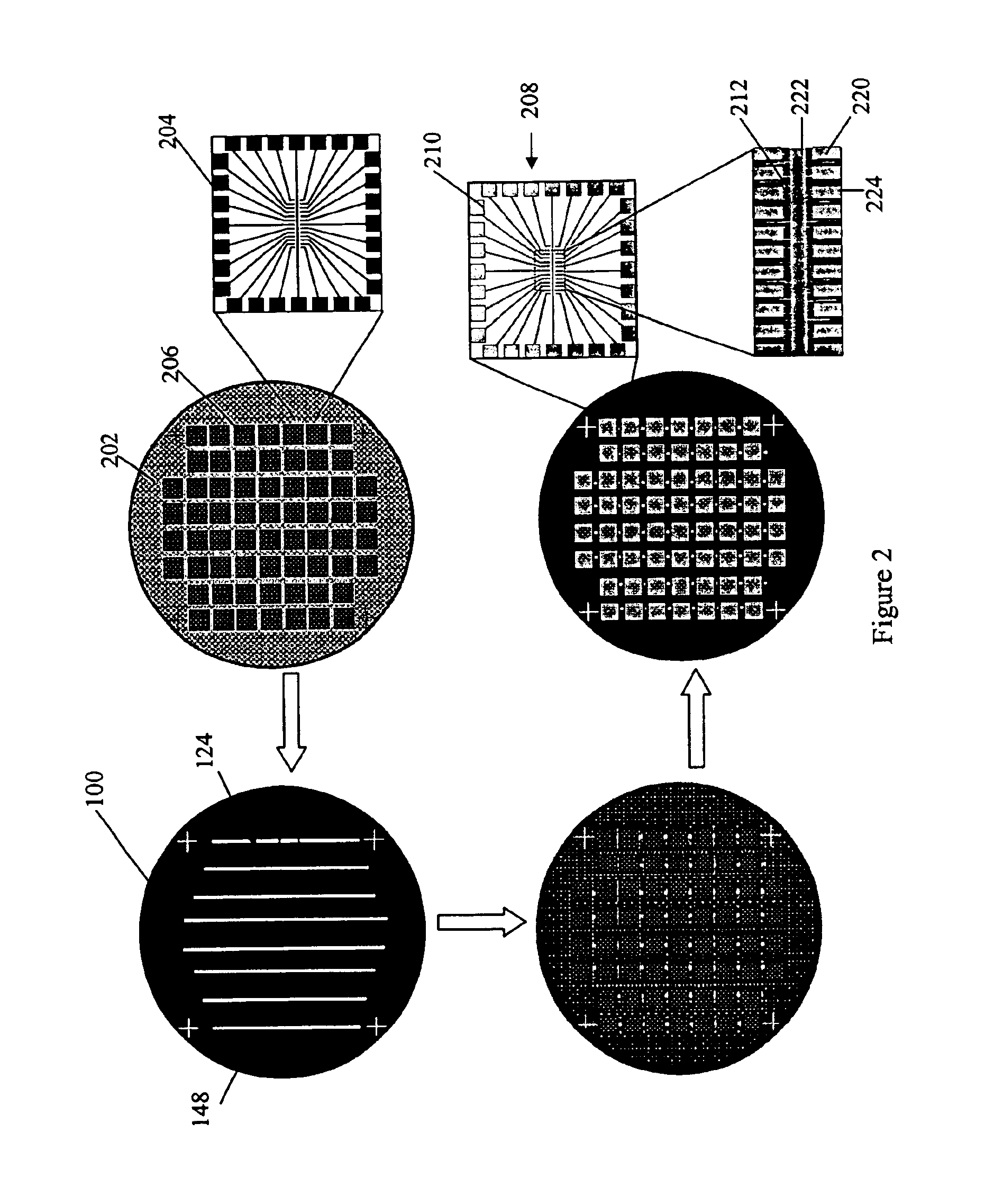
Controlled Positioning and Flow Alignment of Nanowires on a Wafer Scale

Nanowires were positioned and oriented on a substrate and subsequently integrated with electrical connections in accordance with the invention.

Silicon nanowires used for flow alignment were synthesized by gold cluster mediated chemical vapor deposition methods, and the resulting nanowires were suspended in ethanol solution via ultrasonication.

A poly(dimethylsiloxane) (PDMS) stamp, e.g., as shown in FIG. 1, was fabricated by photolithography. The PDMS stamp had a three-inch diameter, with eight parallel channels spaced 7 mm apart with each channel having a width of 500 μm, and a depth of ˜200 μm.

A silicon substrate wafer (surface oxidized, 600 nm oxide) to be used in flow assembly was functionalized with an NH2-terminated self-assembled monolayer (SAM) by immersion in a 1 mM chloroform solution of 3-aminopropyltriethoxysilane (APTES) for 30 min, followed by heating at 110° C. for 10 min.

Alignment of nanowires was ...


PUM

PropertyMeasurementUnit
distanceaaaaaaaaaa
distanceaaaaaaaaaa
length:widthaaaaaaaaaa

Abstract

Methods of positioning and orienting nanostructures, and particularly nanowires, on surfaces for subsequent use or integration. The methods utilize mask based processes alone or in combination with flow based alignment of the nanostructures to provide oriented and positioned nanostructures on surfaces. Also provided are populations of positioned and/or oriented nanostructures, devices that include populations of positioned and/or oriented nanostructures, systems for positioning and/or orienting nanostructures, and related devices, systems and methods.

Description

BACKGROUND OF THE INVENTIONNanotubes, nanocrystals, nanowires, and particularly semiconductor nanowires have gained a great deal of attention for their interesting and novel properties in electrical, chemical, optical and other applications. Such nanomaterials have a wide variety of expected and actual uses, including use as semiconductors for nanoscale electronics, optoelectronic applications in emissive devices, e.g., nanolasers, LEDs, etc., photovoltaics, and sensor applications, e.g., as nano-ChemFETS.While commercial applications of the molecular, physical, chemical and optical properties of these materials have been postulated for all of these different types of materials, generating commercially viable products has not, as yet, been forthcoming. In the world of devices with integrated nanomaterial elements, some of the difficulties in producing commercially viable products has stemmed from the difficulty in handling and interfacing with such small scale materials. Specificall...

Claims


Application Information

Patent Timeline
Patent Type & Authority Patents(United States)
IPC IPC(8): H01L51/40H01L51/05H01L51/30B81C99/00C23F1/00
CPCB81C99/008B82B3/00B82Y10/00B82Y30/00B82Y40/00G11B5/743H01L51/0001H01L51/0048H01L51/0595B81C3/005B01J23/52B81B2203/0361H01L2924/0002B81B2207/015G11C2213/81H01L29/7869Y10S977/89Y10S977/762Y10S438/962Y10S977/857Y10S977/856Y10S977/858B81C2203/057H01L2924/00H10K71/00H10K85/221H10K10/701
Inventor DUAN, XIANGFENGDANIELS, HUGHNIU, CHUNMINGSAHI, VIJENDRAHAMILTON, JAMESROMANO, LINDA T.
Owner ONED MATERIAL INC
Why Eureka
Try Eureka