Electron optical system array, method of fabricating the same, charged-particle beam exposure apparatus, and device manufacturing method

a technology of optical system array and electron beam, applied in the direction of beam deviation/focusing by electric/magnetic means, instruments, therapy, etc., can solve the problems of low productivity, low reliability, and low efficiency of fabrication process, and achieve high precision and reliability.

Inactive Publication Date: 2005-03-29
CANON KK
View PDF62 Cites 42 Cited by
  • Summary
  • Abstract
  • Description
  • Claims
  • Application Information

AI Technical Summary

Benefits of technology

[0009]The present invention has been made to overcome the conventional drawbacks, and has as its principal object to provide an improvement of the prior arts. It is an object of the present invention to provide an electron optical system array which realizes various conditions such as downsizing, high precision, and high reliability at high level. It is another object of the present invention to provide a high-precision exposure apparatus using the electron optical system array, a high-productivity device manufacturing method, a semiconductor device production factory, and the like.

Problems solved by technology

This method suffers many problems as a mass-production exposure apparatus because of a low throughput.
This method is advantageous to a simple repetitive pattern but disadvantageous to a random pattern such as a logic interconnection pattern in terms of the throughput, and a low productivity disables practical application.
The fabrication process becomes difficult at a small electrode interval, and the multilayered structure is low in strength.

Method used


Image

  • Electron optical system array, method of fabricating the same, charged-particle beam exposure apparatus, and device manufacturing method
  • Electron optical system array, method of fabricating the same, charged-particle beam exposure apparatus, and device manufacturing method
  • Electron optical system array, method of fabricating the same, charged-particle beam exposure apparatus, and device manufacturing method

Examples


first embodiment

[0050

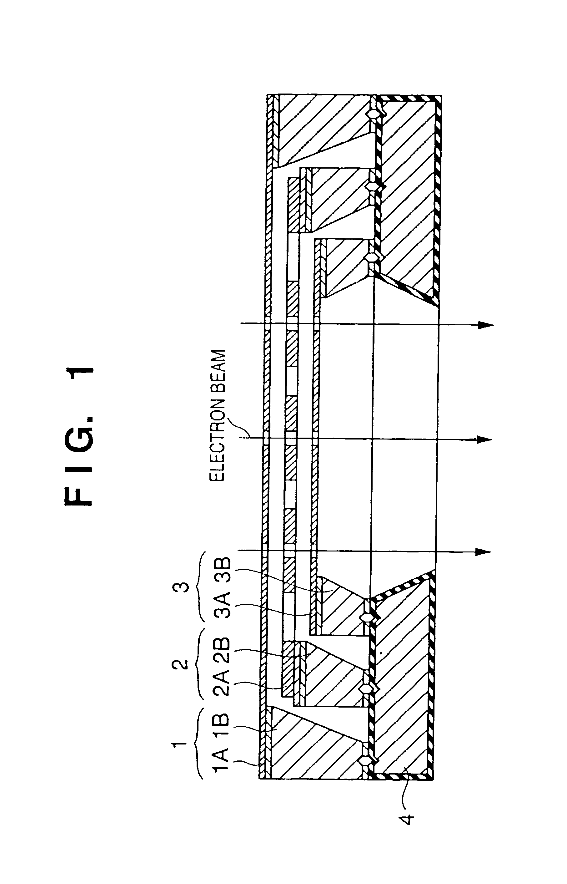
[0051]An electron optical system array according to the first embodiment of the present invention will be described with reference to FIG. 1. In this electron optical system array, upper, middle, and lower electrodes 1, 2, and 3 have a nested structure and are supported by the same surface of a base substrate 4. That is, the electron optical system array comprises the first, second, and third electrodes 1, 2, and 3 respectively having membranes 1A, 2A, and 3A in which a plurality of apertures are formed on the paths of a plurality of electron beams (charged-particle beams), and support substrates 1B, 2B, and 3B which support corresponding membranes. These membranes are spatially insulated. The support substrates of the first to third electrodes are held by the single base substrate 4. The three electrodes form a nested structure such that the support substrate 2B of the second electrode 2 is located inside the support substrate 1B of the first electrode 1 and the support substr...

second embodiment

[0068

[0069]FIG. 5 is a sectional view showing an electron optical system array according to the second embodiment of the present invention. In this electron optical system array, middle and lower electrodes 12 and 13 are fixed to a base substrate 14 to form a nested structure, whereas an upper electrode 11 is fixed to the middle electrode 12 without nesting. The upper and middle electrodes 11 and 12 are fixed with an adhesive 16 via spacers 15 such as fibers, and the outer size of the spacer 15 determines the substrate interval. In FIG. 5, reference numerals 11A, 12A, and 13A denote membranes of the upper, middle, and lower electrodes 11, 12, and 13, respectively; and 11B, 12B, and 13B, membrane support substrates of the upper, middle, and lower electrodes 11, 12, and 13.

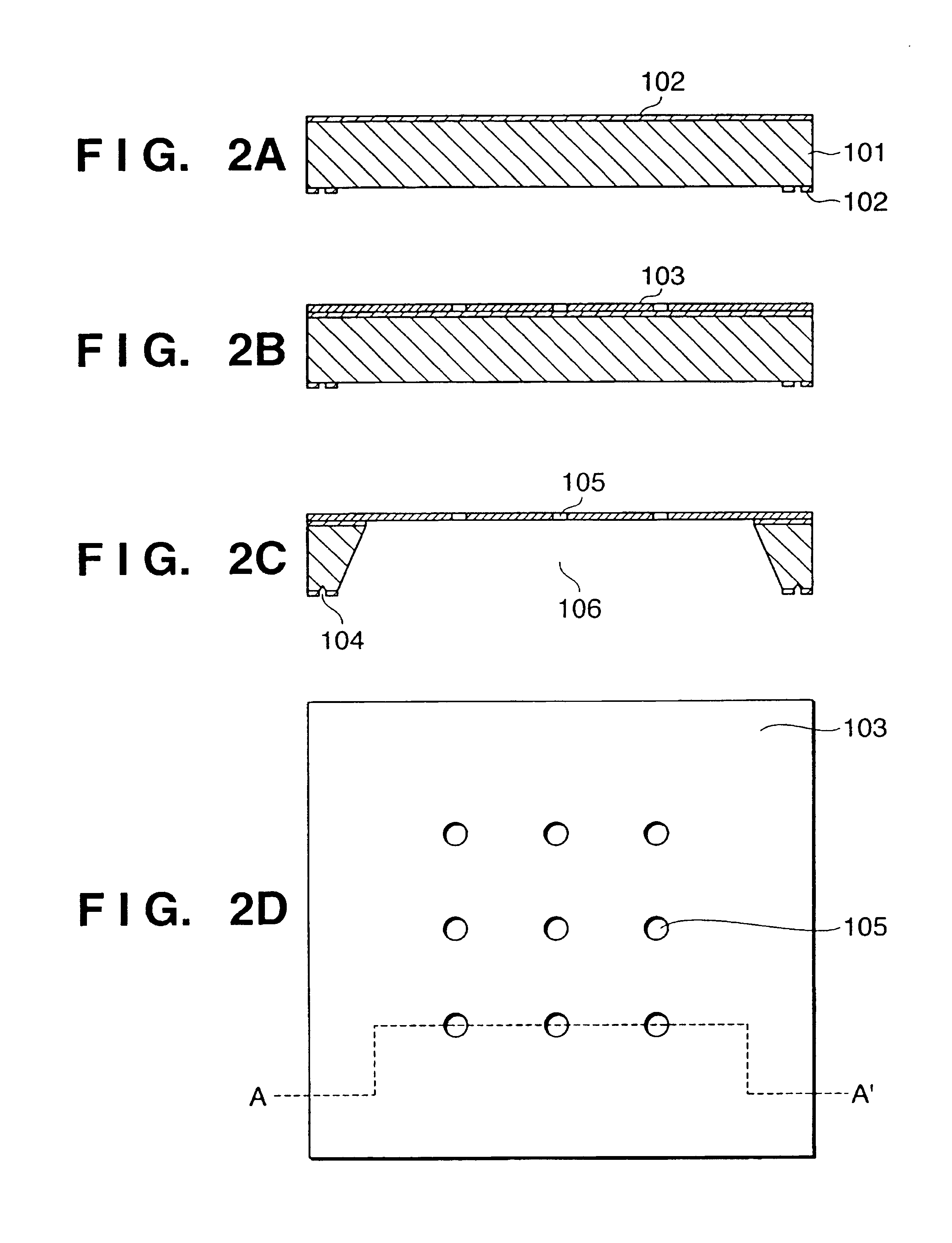
[0070]FIGS. 6A to 6F show a method of forming the upper and lower electrodes 11 and 13. For descriptive convenience, the method of forming the upper and lower electrodes 11 and 13 will be explained with reference to...

third embodiment

[0081

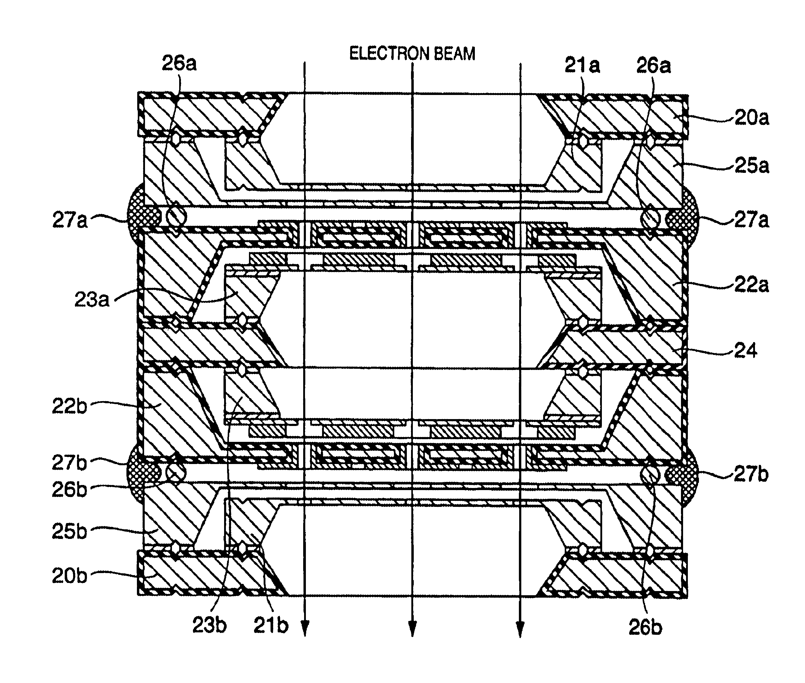
[0082]FIG. 8 is a sectional view showing an electron optical system array according to the third embodiment of the present invention. This electron optical system array employs a shield electrode 25 between upper and middle electrodes 21 and 22. More specifically, the electron optical system array has two units respectively made up of the upper electrode 21 and shield electrode 25 of a nested structure that are fixed to a base substrate 20, and a lower electrode 23 and the middle electrode 22 that are fixed to a base substrate 24. These units are fixed with an adhesive 27 via spacers 26. In FIG. 8, reference numerals 21A, 22A, 23A, and 25A denote membranes of the upper, middle, lower, and shield electrodes 21, 22, 23, and 25, respectively; and 21B, 22B, 23B, and 25B, membrane support substrates of the upper, middle, lower, and shield electrodes 21, 22, 23, and 25.

[0083]FIGS. 9A to 9F are views for explaining a method of forming the middle electrode 22. A silicon wafer 601 of th...


PUM

PropertyMeasurementUnit
widthaaaaaaaaaa
thicknessesaaaaaaaaaa

Abstract

This invention relates to an electron optical system array having a plurality of electron lenses. The electron optical system array includes a plurality of electrodes arranged along the paths of a plurality of charged-particle beams. Each of the plurality of electrodes has a membrane in which a plurality of apertures are formed on the paths of the plurality of charged-particle beams, and a support portion which supports the membrane. At least two of the plurality of electrodes are arranged to form a nested structure.

Description

FIELD OF THE INVENTION[0002]The present invention relates to an electron optical system array suitable for an exposure apparatus using charged-particle beams such as electron beams and, more particularly, to an electron optical system array having a plurality of electron lenses.BACKGROUND OF THE INVENTION[0003]In production of semiconductor devices, an electron beam exposure technique receives a great deal of attention as a promising candidate of lithography capable of micro-pattern exposure at a line width of 0.1 μm or less. There are several electron beam exposure methods. An example is a variable rectangular beam method of drawing a pattern with one stroke. This method suffers many problems as a mass-production exposure apparatus because of a low throughput. To attain a high throughput, there is proposed a pattern projection method of reducing and transferring a pattern formed on a stencil mask. This method is advantageous to a simple repetitive pattern but disadvantageous to a r...

Claims


Application Information

Patent Timeline
Patent Type & Authority Patents(United States)
IPC IPC(8): H01J37/12H01J37/10H01J37/305G03F7/20H01J37/317H01L21/027
CPCB82Y10/00B82Y40/00H01J37/3174H01J37/12H01J2237/1205
Inventor SHIMADA, YASUHIROYAGI, TAKAYUKIONO, HARUHITO
Owner CANON KK
Why Eureka
Try Eureka