Semiconductor substrate with stacked oxide and SOI layers with a molten or epitaxial layer formed on an edge of the stacked layers

Inactive Publication Date: 2005-03-29
RENESAS ELECTRONICS CORP
View PDF21 Cites 13 Cited by
  • Summary
  • Abstract
  • Description
  • Claims
  • Application Information

AI Technical Summary

Benefits of technology

[0048]According to the semiconductor substrate processing method of the fifth aspect of the present invention, the thickness of the thickest part of the insulating film is set to be equal to or larger than the total thickness of the buried oxide film and the SOI layer so that the curved part of the buried oxide film is formed inside the insulating film. This prevents formation of the curved part of the buried oxide film in the edge part of the semiconductor substrate. Further, since the insulating film is formed as a thermal oxide film, it can easily be obtained with a suppressed increase in production cost due to the application of the invention.
[0049]According to the semiconductor substrate processing method of the sixth aspect of the present invention, the thickness of the thickest part of the insulating film is set to be equal to or larger than the total thickness of the buried oxide film and the SOI layer so that the curved part of the buried oxide film is formed inside the insulating film. This prevents formation of the curved part of the buried oxide film in the edge part of the semiconductor substrate. Further, the insulating film is formed as a TEOS film, a good insulating film having less pinholes.
[0050]According to the semiconductor substrate processing method of seventh aspect of the present invention, a protective oxide film is formed in the edge part on, at least, the first main surface side from the surface to the inside. This prevents formation of a thin SOI layer on the buried oxide film in the edge part. In the process of thinning the SOI layer, for example, this prevents the problem that a thin SOI layer is partially surrounded by the buried oxide film and an oxide film formed for the thinning process, partially lifted off in removal of the oxide film to be particles, and suspended in etching solution. This in turn prevents defective

Problems solved by technology

While SOI (Silicon On Insulator) devices in which semiconductor elements are formed on SOI substrates are superior to bulk devices in their reduced junction capacitance and improved element isolation breakdown voltage, the SOI devices have their unique problems as described below.
Further, the surface of the edge part is not smooth but rough with irregularities.
If particles adhere to

Method used


Image

  • Semiconductor substrate with stacked oxide and SOI layers with a molten or epitaxial layer formed on an edge of the stacked layers
  • Semiconductor substrate with stacked oxide and SOI layers with a molten or epitaxial layer formed on an edge of the stacked layers
  • Semiconductor substrate with stacked oxide and SOI layers with a molten or epitaxial layer formed on an edge of the stacked layers

Examples


Embodiment Construction

A. First Preferred Embodiment

[0088]A semiconductor substrate processing method and a semiconductor substrate according to a first preferred embodiment of the present invention will now be described referring to FIG. 1 to FIG. 4. In the following description, a semiconductor substrate is referred to separately in its upper main surface (the side on which semiconductor elements are formed), center part thereof (including the active region in which semiconductor elements are actually formed), edge part including the peripheral part around the center part and the side, and lower main surface.

[0089]

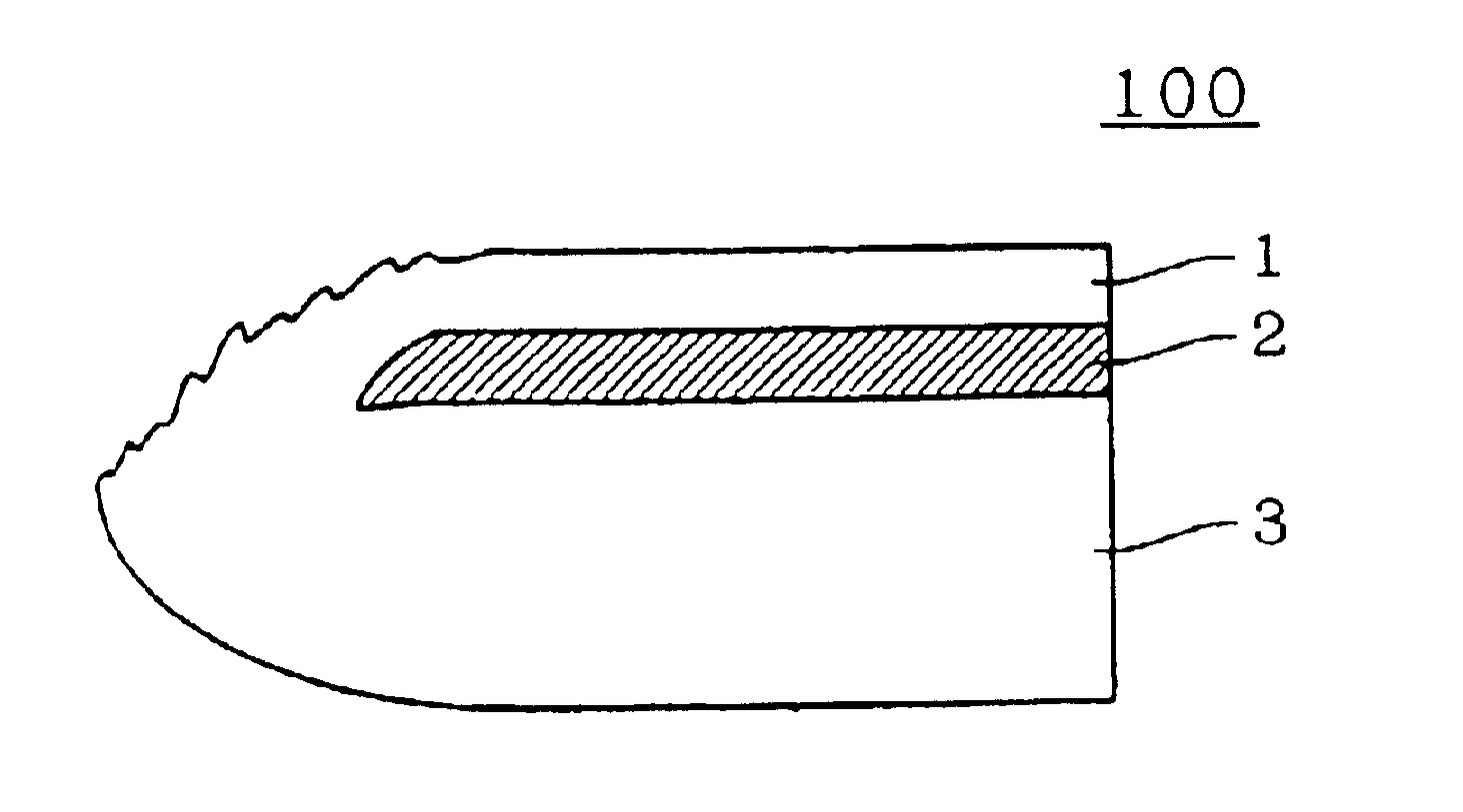
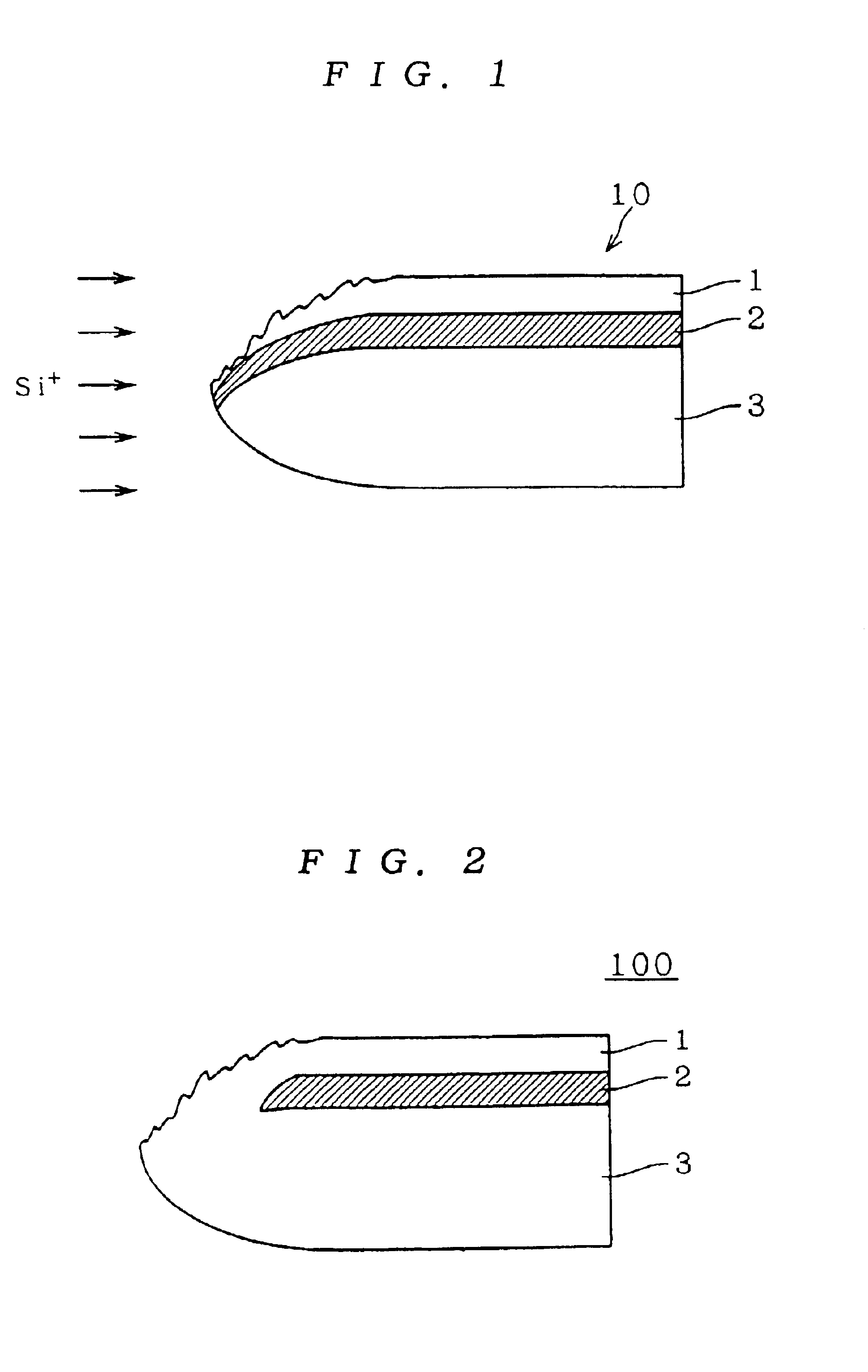
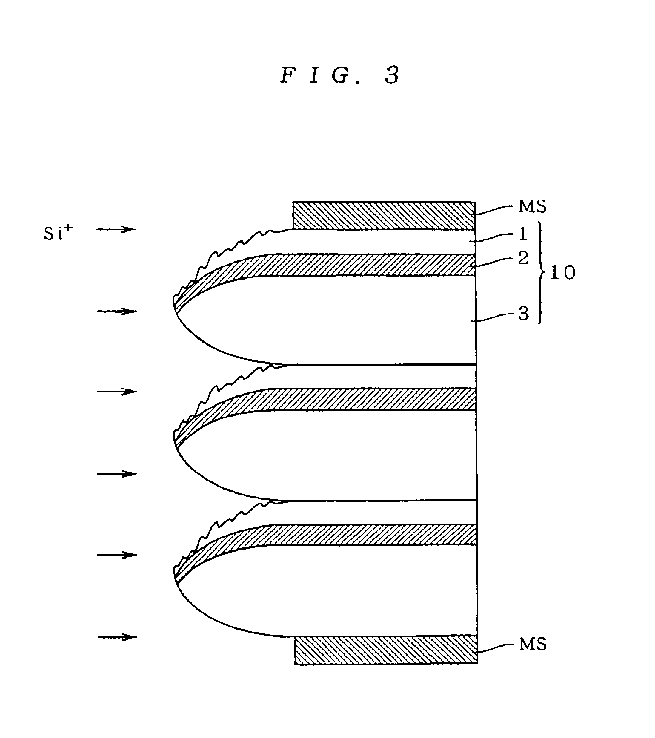
[0090]FIG. 1 is a diagram showing a partial section of an SOI substrate 10 formed by an SIMOX (Separation by Implanted Oxygen) method. In the SIMOX method, an SOI structure is obtained by implanting oxygen ions to doses of 1×10¹⁸ to 2×10¹⁸ / cm2 at 150 to 200 KeV and then annealing it at about 1300 to 1400° C. The SOI substrate 10 includes a buried oxide film 2 and a single-crystal silicon layer...


PUM


Abstract

A semiconductor substrate that prevents formation of particles from an edge part of the substrate. The substrate contains an on-substrate oxide film and an SOI layer stacked on the oxide film. A molten layer is formed on the edge part of the on-substrate oxide film and the SOI layer by mixing the SOI layer and the on-substrate oxide film to cover the edge part. An epitaxial layer may also be formed on the edge part of the on-substrate oxide film and the SOI layer to cover the edge part.

Description

[0002]This application is a divisional of application Ser. No. 09 / 770,388, filed Jan. 29, 2001, now U.S. Pat. No. 6,563,172, which is itself a divisional of application Ser. No. 09 / 113,155, filed Jul. 10, 1998, now U.S. Pat. No. 6,232,201. This application claims priority under 35 U.S.C. §119(a)-(d) to Japanese Patent Application No. 10-4980, filed Jan. 13, 1998. The contents of applications 09 / 113,155 and 09 / 770,388, and Japanese Patent Application No. 10-4980 are herein incorporated by reference.BACKGROUND OF THE INVENTION[0003]1. Field of the Invention[0004]The present invention relates to methods for processing semiconductor substrates and the semiconductor substrates, and particularly to a semiconductor substrate processing method and a semiconductor substrate in which formation of dust particles from the edge part of the substrate is prevented.[0005]2. Description of the Background Art[0006]While SOI (Silicon On Insulator) devices in which semiconductor elements are formed on ...

Claims


Application Information

Patent Timeline
IPC IPC(8): H01L21/70H01L21/762H01L21/02H01L21/3105H01L21/3115H01L21/265H01L27/12
CPCH01L21/3105H01L21/7624H01L21/31155H01L27/12
Inventor YOSHIDA, YOSHIKONARUOKA, HIDEKIKIMURA, YASUHIROYAMAGUCHI, YASUOIWAMATSU, TOSHIAKIHIRANO, YUUICHI
Owner RENESAS ELECTRONICS CORP
Why Eureka
Try Eureka