Semiconductor wafer cleaning systems and methods

a technology of semiconductor wafers and cleaning systems, applied in the direction of cleaning using liquids, furniture, instruments, etc., can solve the problems of less than a full set of processing, less and less effective processing, and unsuitable wafer proportions, etc., to reduce the use of enhancement substances and reduce processing liquids

Inactive Publication Date: 2005-04-05
TEL EPION
View PDF37 Cites 37 Cited by
  • Summary
  • Abstract
  • Description
  • Claims
  • Application Information

AI Technical Summary

Benefits of technology

The present invention overcomes the deficiencies and shortcomings of the prior art by providing an immersion processing system for cleaning wafers that increases the efficiency of chemical use. Such a system advantageously uses less cleaning enhancement substance that may be provided as gas, vapor or liquid directly to a meniscus or wafer / liquid / gas bath interface so as to effectively modify surface tensions at the meniscus with minimized chemical usage.
A method in accordance with this aspect includes the steps of providing a plurality of immersion vessels containing a liquid bath, immersing at least a portion of a surface of a microelectronic device within the liquid bath of one of the plurality of the immersion vessels while immersing at least a portion of a surface of another of the plurality of microelectronic devices within a different immersion vessel, separating the microelectronic devices from their respective liquid baths and forming meniscus at interfaces between a surface of each microelectronic device and its respective liquid bath, and, for each of the plurality of microelectronic devices, delivering cleaning enhancement substance to the meniscus between the surface and the liquid bath that is formed while the microelectronic device is separated from the liquid bath. A significant further advantage of such an arrangement and method of processing is that any number of such independent vessels can be arranged together in an array, for example, of any size. That is, such an arrangement and method are totally scalable depending on application needs. Furthermore, such an arrangement permits a usage of less than all of the vessels so that one or any number up to the arrangement number vessels can be used for any particular need, thus reducing the processing liquid and cleaning enhancement substance usage also by only using the vessels that are needed for a particular need. Thus, even a single wafer can be processed without the need to run a whole batch process.

Problems solved by technology

If such droplets or films are left to evaporate from the wafer surface, any contaminants within the droplets or films will be deposited on the wafer surface, which contaminants may render a portion of the wafer unsuitable for further processing or use.
However, minute liquid droplets or films are sometimes very difficult to remove due to their attraction to the wafer surfaces.
However, such chemical use effectiveness is based upon the processing of a full set of wafers at all times. Processing of less than a full set becomes less and less effective because the vessels themselves contain the same volumes that must be filled by processing liquids as well as processing gases, thereby increasing the volume of process fluids and gases used per wafer processed.

Method used


Image

  • Semiconductor wafer cleaning systems and methods
  • Semiconductor wafer cleaning systems and methods
  • Semiconductor wafer cleaning systems and methods

Examples


examples

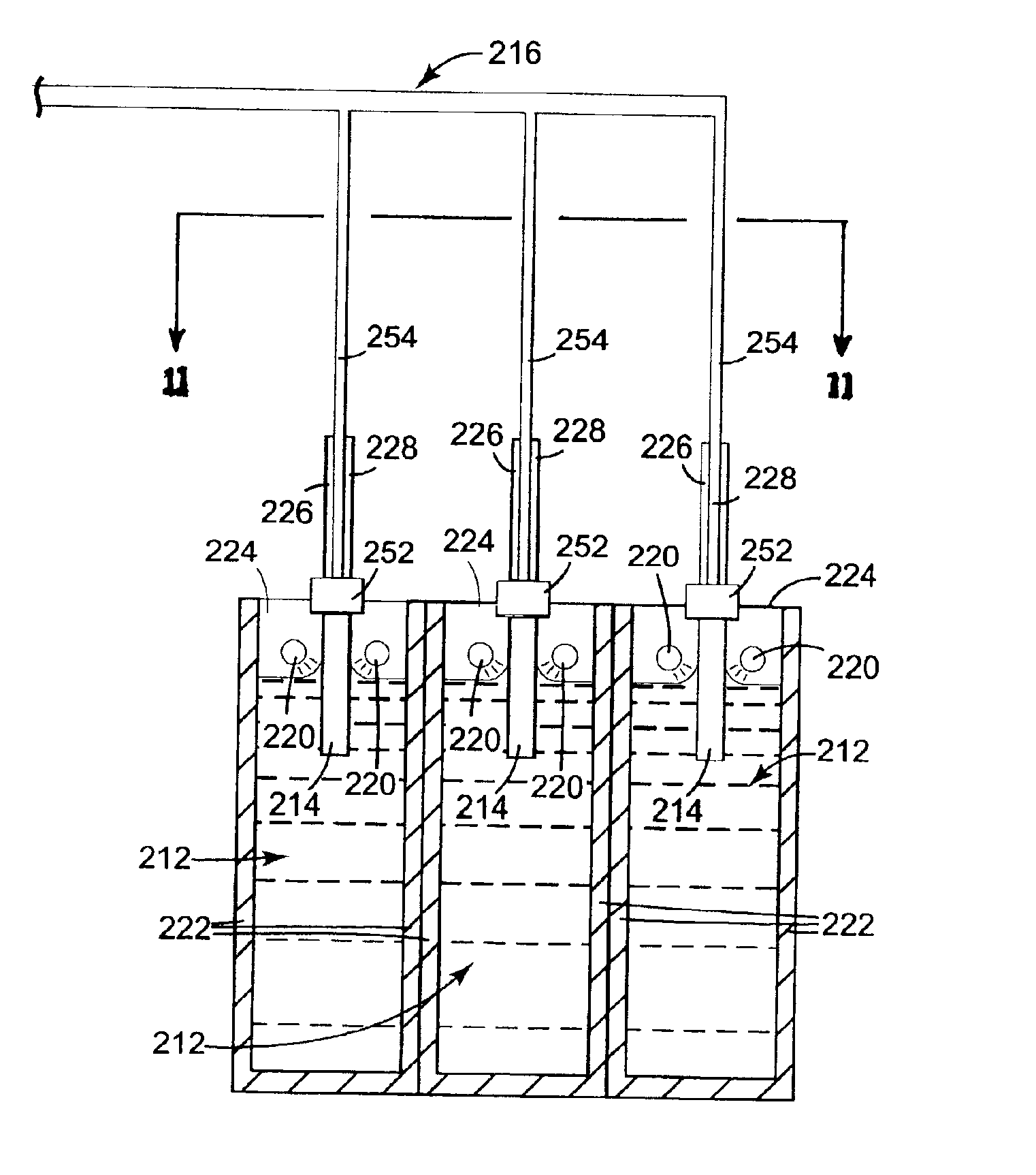
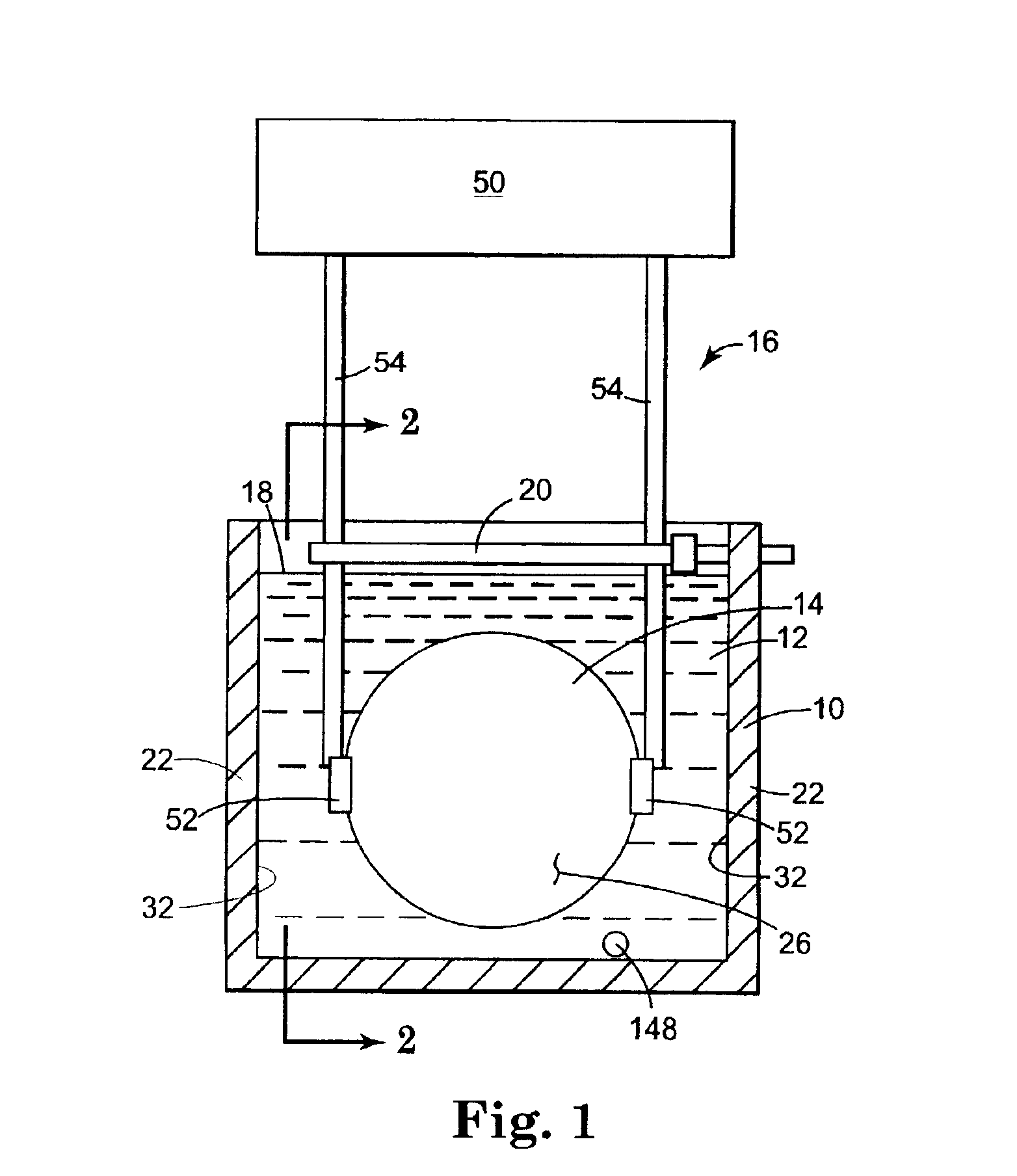
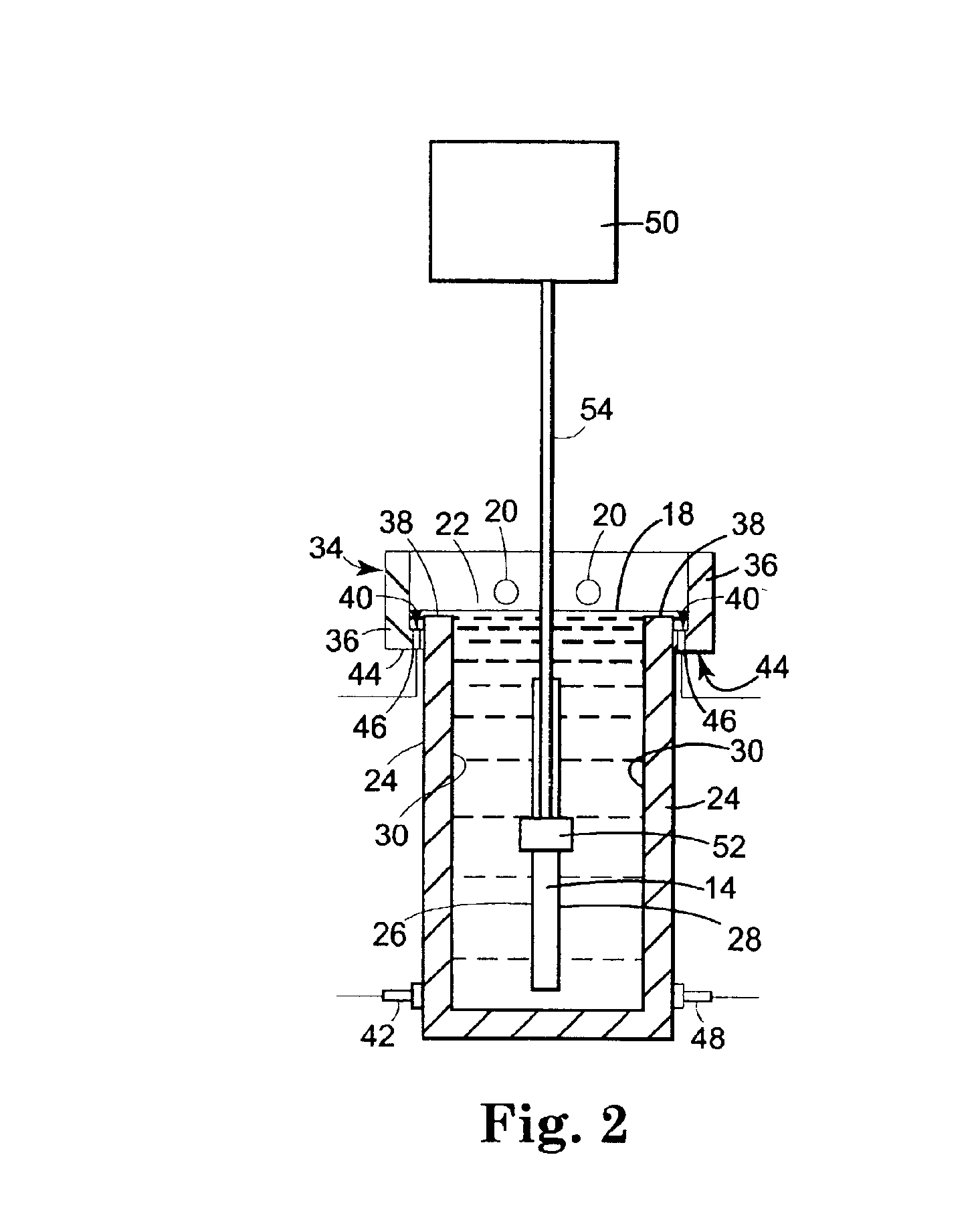
Wafer cleaning experiments were conducted on 200 mm diameter, 0.75 mm thick silicon wafers in a single-wafer vessel similar to that shown in FIGS. 1 through 5. The wafer was vertically oriented and centered horizontally in a rectangular, 265 mm wide by 8 mm deep by 265 mm high vessel cavity. The process cavity was formed by machining two 1″ polyvinylidine fluoride (PVDF) sheets and welding them together at the sides and bottom. Liquid entered the cavity through holes in the side walls near the bottom of the vessel.

The outer vessels spanned the full width of the side walls, were constructed of ⅛″ PVDF, and formed a 49 mm wide by 70 mm high channel to catch the overflow from the inner vessel. The weir consisted of 18 mm thick PVDF plate angled at 45°. There was a series of 3 mm deep v-grooves with a 60° included angle cut at a 4.75 mm pitch across the full width of each weir.

Semiconductor grade, ultrapure deionized water (DI water) was used as the process liquid and semiconductor grad...


PUM

PropertyMeasurementUnit
diameteraaaaaaaaaa
diameteraaaaaaaaaa
widthaaaaaaaaaa

Abstract

An immersion processing system is provided for cleaning wafers with an increased efficiency of chemical use. Such a system advantageously uses less cleaning enhancement substance that may be provided as gas, vapor or liquid directly to a meniscus or wafer / liquid / gas bath interface so as to effectively modify surface tensions at the meniscus with minimized chemical usage. Such a delivery system design may be applied for single wafer processing or for processing multiple wafers together within a single liquid bath vessel. For single wafer processing, in particular, cleaning enhancement substance can be delivered along one or both major sides of the wafer, preferably at the meniscus that is formed as the wafer and liquid are relatively moved, while a processing vessel usable for such single wafer processing may itself be designed with a minimized size to accommodate a single wafer. By reducing the vessel volume, chemical usage for any processing chemicals that are to be provided within a liquid bath may also be advantageously reduced.

Description

FIELD OF THE INVENTIONThe present invention relates to the wet processing and cleaning of semiconductor wafers within a liquid bath and the subsequent separation of wafers from the liquid bath while cleaning wafer surfaces. In particular, the present invention relates to separation of one or more wafers from a liquid bath after wet processing while providing a cleaning enhancement substance to an object / liquid / gas interface for enhanced surface cleaning.BACKGROUND OF THE PRESENT INVENTIONWet processing of many types of objects often includes a step of separating the object from the liquid as either a finished product or for further processing. Moreover, it is often desirable to rinse and / or clean the object after wet processing to remove any contaminants or left over and unwanted processing liquids and to provide a clean processed object. Also, in many cases, depending on any further treatment or handling, the object may be further dried to remove any processing or rinsing liquids t...

Claims


Application Information

Patent Timeline
Patent Type & Authority Patents(United States)
IPC IPC(8): B08B3/04B08B3/10B08B5/02H01L21/00G11B23/50
CPCB08B3/04B08B3/10H01L21/67057H01L21/67051B08B5/02G11B23/505
Inventor CHRISTENSON, KURT K.RATHMAN, CHRISTINA A.
Owner TEL EPION
Why Eureka
Try Eureka