Combined E-beam and optical exposure semiconductor lithography

a semiconductor and lithography technology, applied in semiconductor/solid-state device testing/measurement, semiconductor/solid-state device details, instruments, etc., can solve the problems of relative fast and less precise, achieve high throughput and yield, and improve the accuracy of lithography results

Inactive Publication Date: 2005-04-05
TAIWAN SEMICON MFG CO LTD
View PDF33 Cites 10 Cited by
  • Summary
  • Abstract
  • Description
  • Claims
  • Application Information

AI Technical Summary

Benefits of technology

Embodiments of the invention provide for advantages over the prior art. The relatively small number of CD areas of a semiconductor design are transferred to a semiconductor wafer by the relatively slow, but highly precise, process of e-beam writing. Conversely, the relatively large number of non-CD areas of the semiconductor design are transferred to the wafer by the relatively fast, but less precise, process of optical exposure lithography. Therefore, the CD's of the semiconductor design are properly transferred to the wafer, while still for the most part ensuring the high throughput and yield that are characteristics of optical exposure lithography. That is, e-beam writing is used only as is necessary. Thus, the combination of e-beam writing and optical exposure is used on the same wafer to obtain good resolution and depth of focus (DOF) via the e-beam writing, and also to obtain to high throughput of optical exposure.

Problems solved by technology

Conversely, the relatively large number of non-CD areas of the semiconductor design are transferred to the wafer by the relatively fast, but less precise, process of optical exposure lithography.

Method used


Image

  • Combined E-beam and optical exposure semiconductor lithography
  • Combined E-beam and optical exposure semiconductor lithography
  • Combined E-beam and optical exposure semiconductor lithography

Examples


Embodiment Construction

In the following detailed description of exemplary embodiments of the invention, reference is made to the accompanying drawings that form a part hereof, and in which is shown by way of illustration specific exemplary embodiments in which the invention may be practiced. These embodiments are described in sufficient detail to enable those skilled in the art to practice the invention. Other embodiments may be utilized, and logical, mechanical, and other changes may be made without departing from the spirit or scope of the present invention. The following detailed description is, therefore, not to be taken in a limiting sense, and the scope of the present invention is defined only by the appended claims.

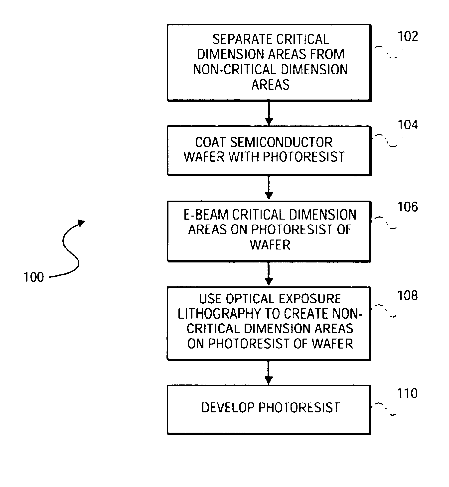
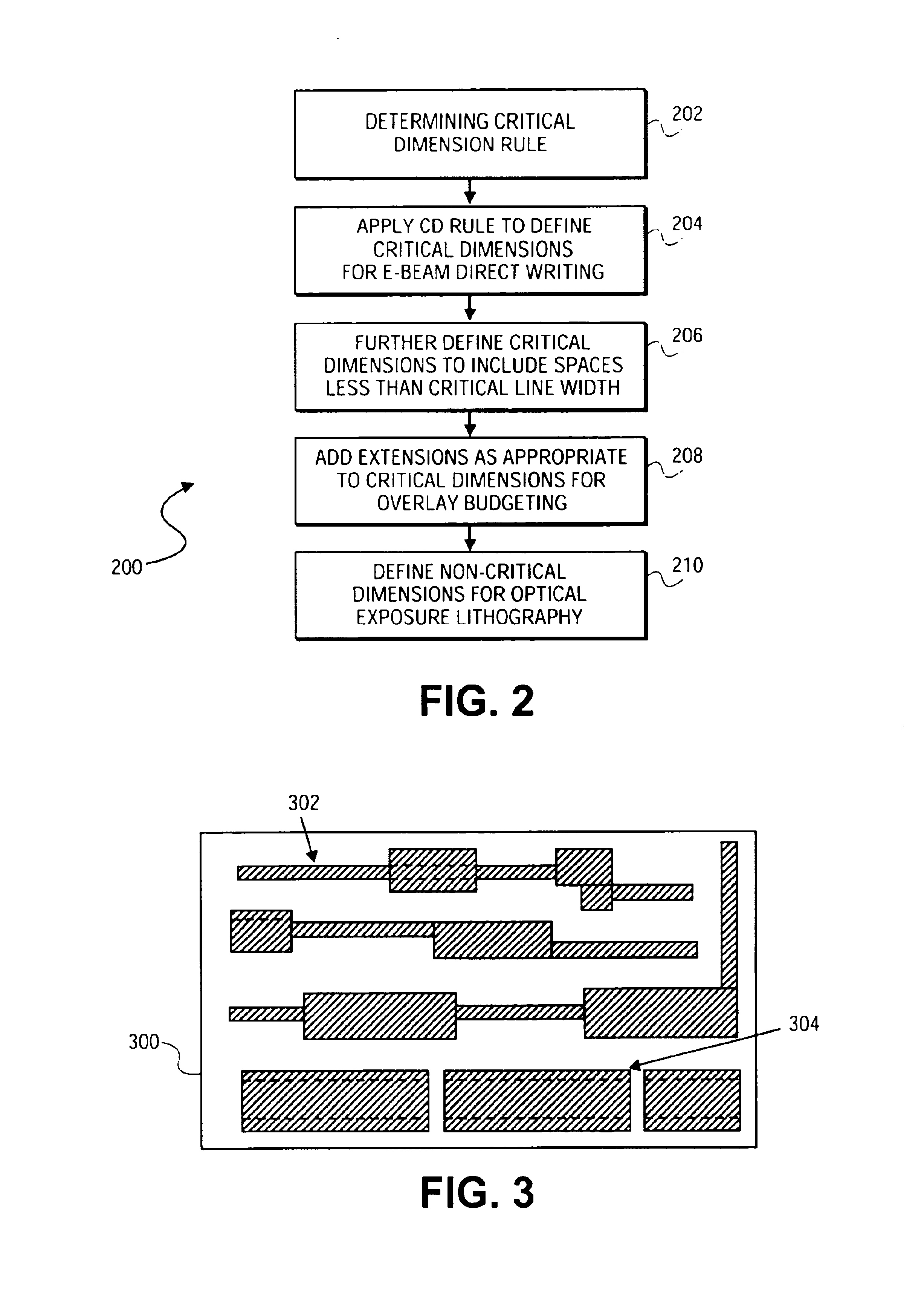
FIG. 1 shows a method 100 in accordance with which one embodiment fabricates semiconductor devices according to a semiconductor design on a semiconductor wafer. Critical dimension (CD) areas of the semiconductor design are first separated from non-CD areas of the semiconductor design (10...


PUM

PropertyMeasurementUnit
sizesaaaaaaaaaa
sizesaaaaaaaaaa
wavelengthsaaaaaaaaaa

Abstract

Combined e-beam and optical exposure lithography for semiconductor fabrication is disclosed. E-beam direct writing to is employed to create critical dimension (CD) areas of a semiconductor design on a semiconductor wafer. Optical exposure lithography is employed to create non-CD areas of the semiconductor design on the semiconductor CD's of the semiconductor design can also be separated from non-CD's of the semiconductor design prior to employing e-beam direct writing and optical exposure lithography.

Description

FIELD OF THE INVENTIONThis invention relates generally to semiconductor fabrication, and more particularly to semiconductor lithography as can be performed in such fabrication.BACKGROUND OF THE INVENTIONSince the invention of the integrated circuit (IC), semiconductor chip features have become exponentially smaller and the number of transistors per device exponentially larger. Advanced IC's with hundreds of millions of transistors at feature sizes of 0.25 micron, 0.18 micron, and less are becoming routine. Improvement in overlay tolerances in optical photolithography, and the introduction of new light sources with progressively shorter wavelengths, have allowed optical steppers to significantly reduce the resolution limit for semiconductor fabrication far beyond one micron. To continue to make chip features smaller, and increase the transistor density of semiconductor devices, IC's have begun to be manufactured that have features smaller than the lithographic wavelength.Sub-waveleng...

Claims


Application Information

Patent Timeline
Patent Type & Authority Patents(United States)
IPC IPC(8): G03F7/20H01L21/027H01J37/317H01L21/02
CPCB82Y10/00B82Y40/00G03F7/2022H01L21/0277H01J37/3174H01L21/0274G03F7/7045H01J2237/31757
Inventor LIN, CHIN-HSIANG
Owner TAIWAN SEMICON MFG CO LTD
Why Eureka
Try Eureka