Method to control the interfacial layer for deposition of high dielectric constant films

a technology of high dielectric constant and interfacial layer, which is applied in the field of thin film formation, can solve the problems of low dielectric constant, inability to use silicon dioxide interfacial layer as gate dielectric in cmos devices, and inability to achieve the effect of reducing the dielectric constant, and reducing the thickness of the film

Inactive Publication Date: 2005-04-05
SHARP LAB OF AMERICA INC
View PDF3 Cites 410 Cited by
  • Summary
  • Abstract
  • Description
  • Claims
  • Application Information

AI Technical Summary

Problems solved by technology

Because of high direct tunneling currents, SiO2 films thinner than 1.5 nm generally cannot be used as the gate dielectric in CMOS devices.
One problem with using high-k materials is that an interfacial layer of silicon dioxide, or a silicate layer, with a lower dielectric constant forms during standard processing.
Achieving EOT of less than 1.5 nm is very difficult.
However, it is difficult to initiate deposition on hydrogen terminated silicon surfaces.
But, this results in films that are rough with poor uniformity.
Another problem with tetrachloride precursors is the incorporation of residual chlorine in the film.
The chlorine impurities can result in long term reliability and performance issues.
These precursors also have a problem initiating the film deposition on hydrogen terminated silicon surfaces and will incorporate carbon residues in the film.
Large ligands may also take up enough space that steric hindrance will prevent the deposition of a uniform monolayer.
Problems related to the interfacial layer, such as the formation of silicon oxides or silicates, may remain even using metal nitrate precursors.

Method used


Image

  • Method to control the interfacial layer for deposition of high dielectric constant films
  • Method to control the interfacial layer for deposition of high dielectric constant films
  • Method to control the interfacial layer for deposition of high dielectric constant films

Examples


Embodiment Construction

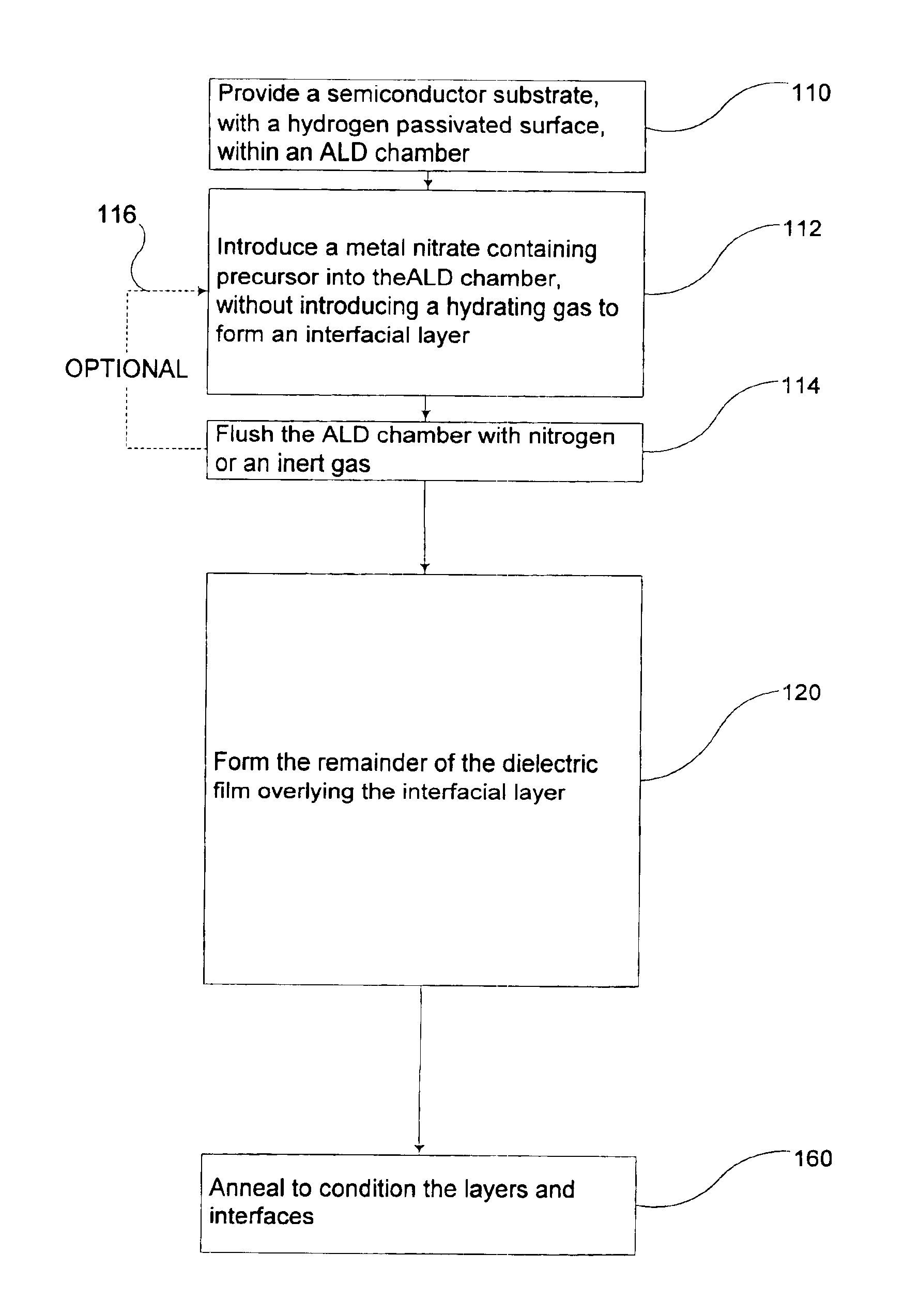
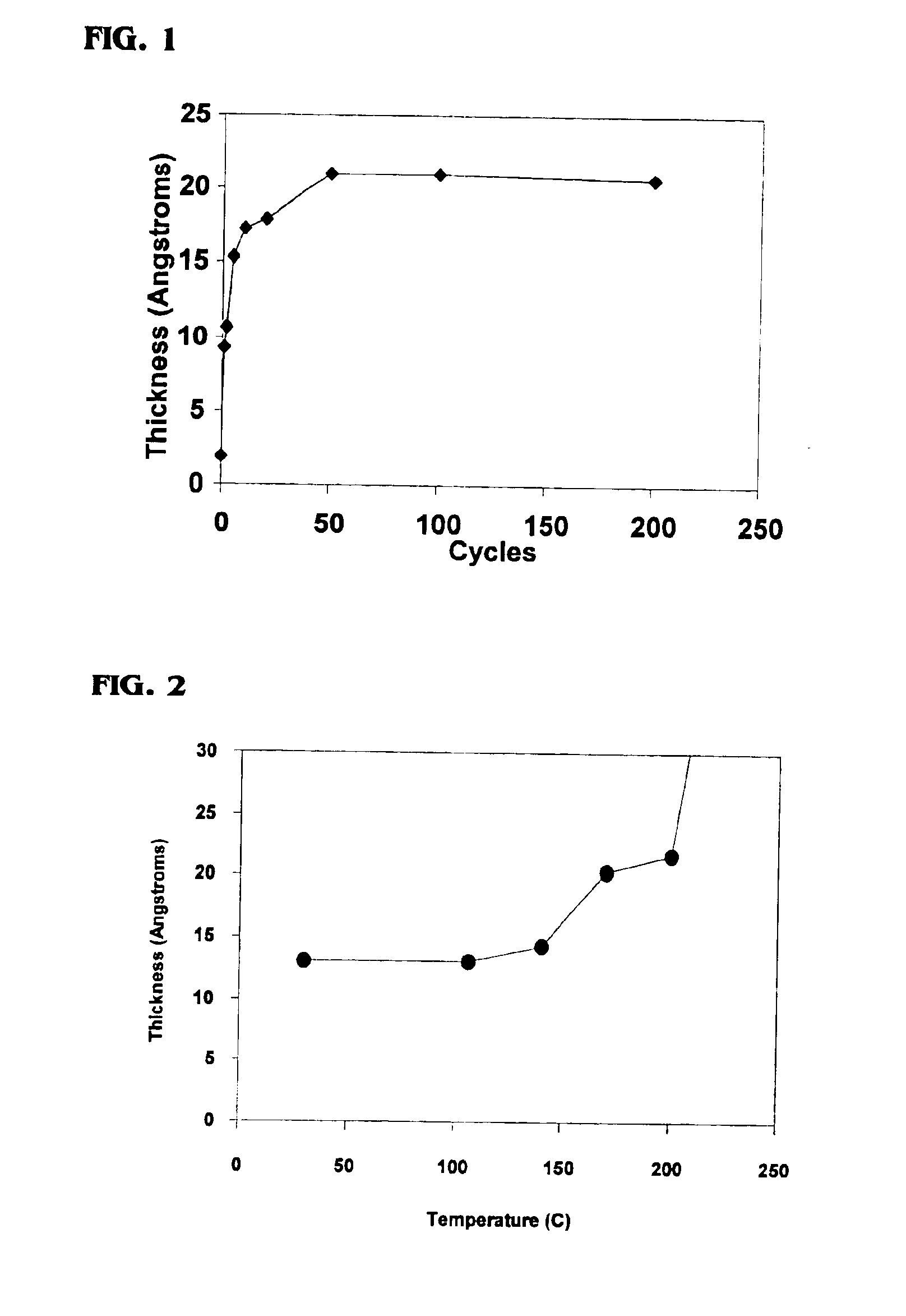
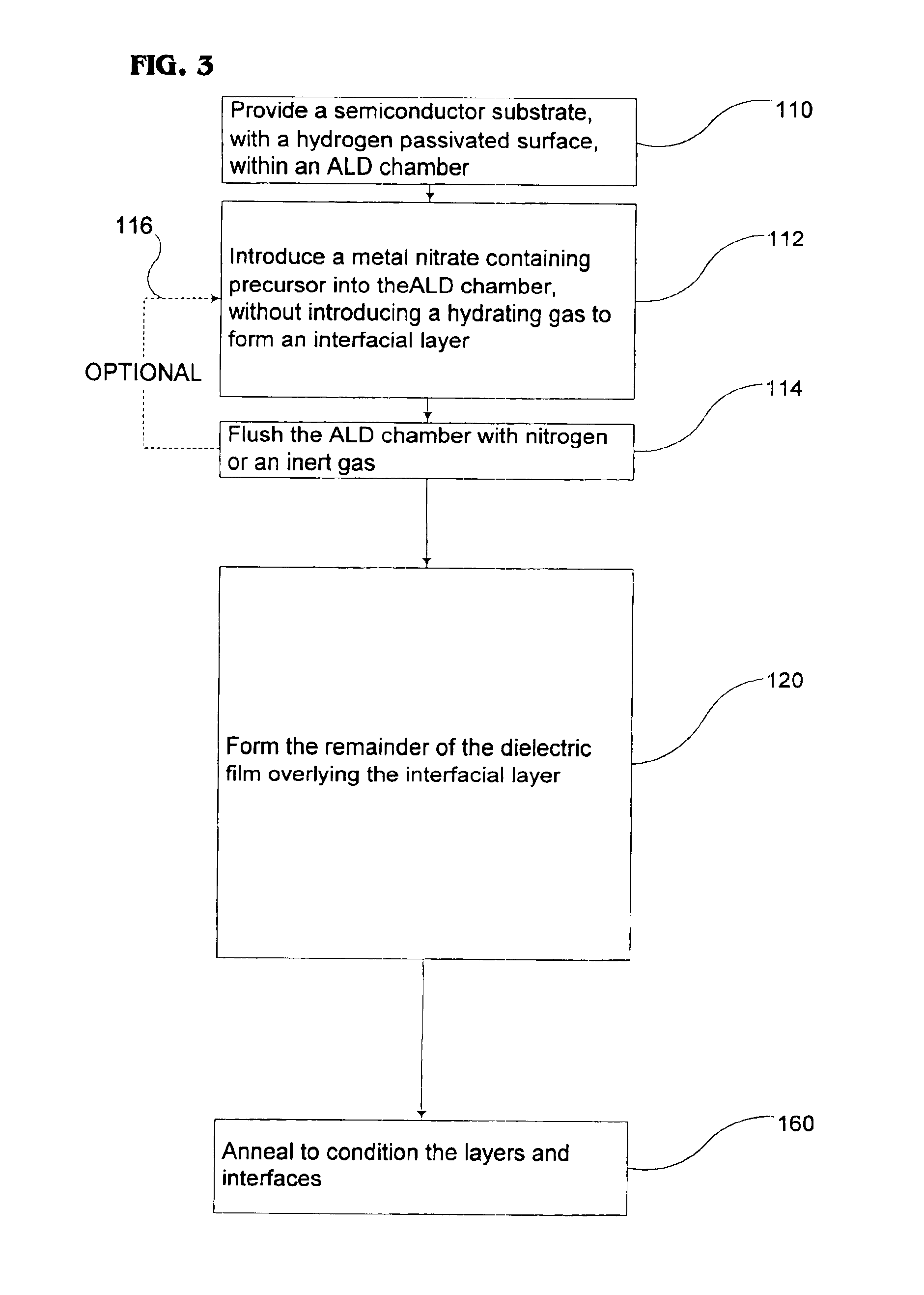
FIG. 1 is a chart showing the film thickness in angstroms of an interfacial layer formed using a M(NO3)x precursor (where M is metal and x is the valence of M), in this example Hf(NO3)4. Generally, M may be Hf, Zr, Gd, La, Ce, Ti, Y, Ta, or Al. The interfacial layer was formed by providing a hydrogen passivated semiconductor surface, in this case hydrogen terminated silicon, in an ALD chamber, and exposing the surface to cycles comprising two seconds of Hf(NO3)4 and ten seconds of N2 at a temperature of approximately 170 degrees Celsius. This interfacial layer initially increases with the number of cycles, but then saturates or self-limits. As shown, using Hf(NO3)4 at 170 degrees Celsius this saturation occurs after about 50 cycles, or 100 seconds total pulse time, of Hf(NO3)4. The interfacial layer shown in FIG. 1 saturates, or self-limits, at between approximately 20 and 22 angstroms. The interfacial layer is preferably a high-k material. A high-k material refers to a material wit...


PUM

PropertyMeasurementUnit
temperatureaaaaaaaaaa
dielectric constantaaaaaaaaaa

Abstract

Methods of forming an interfacial layer on a hydrogen-passivated substrate are provided. These methods utilize atomic layer deposition techniques incorporating metal nitrate-based precursors, such as hafnium nitrate or zirconium nitrate, without introducing a hydrating agent, or oxidizing agent, such as water, during the formation of the interfacial layer. Also provided are methods of forming high-k films, by first forming an interfacial layer on the surface of a hydrogen-passivated substrate, and then depositing one, or more, high-k dielectric films.

Description

BACKGROUND OF THE INVENTIONThe present invention relates generally to methods of forming thin films and, more particularly, to methods of forming high dielectric constant films on hydrogen-passivated substrates.Current Si VLSI technology uses SiO2 as the gate dielectric in MOS devices. As device dimensions continue to scale down, the thickness of the SiO2 layer must also decrease. Thicknesses of less than 1 nanometer (nm) are expected in the future. However, the occurrence of high tunneling current through such thin layers of SiO2 requires that alternate materials be considered. Materials with high dielectric constants would permit gate dielectric layers to be made thicker, and so alleviate the tunneling current problem. These so-called high-k dielectric films are defined herein as having a high dielectric constant relative to silicon dioxide. Typically, silicon dioxide has a dielectric constant of approximately 4, while it would be desirable to use a gate dielectric material with a...

Claims


Application Information

Patent Timeline
Patent Type & Authority Patents(United States)
IPC IPC(8): H01L21/02H01L29/66H01L21/3205H01L29/78H01L21/316C23C16/40C23C16/455H01L21/314
CPCC23C16/405H01L21/3141C23C16/45553H01L21/31645H01L21/02205H01L21/0228H01L21/02304H01L21/02175
Inventor CONLEY, JR., JOHN F.ONO, YOSHI
Owner SHARP LAB OF AMERICA INC
Why Eureka
Try Eureka