Metal-insulator-metal capacitor and method of fabrication
a technology of metal-insulator and capacitor, applied in the direction of capacitor, semiconductor device, semiconductor/solid-state device details, etc., can solve problems such as yield or reliability problems
- Summary
- Abstract
- Description
- Claims
- Application Information
AI Technical Summary
Benefits of technology
Problems solved by technology
Method used
Image

Examples
first embodiment
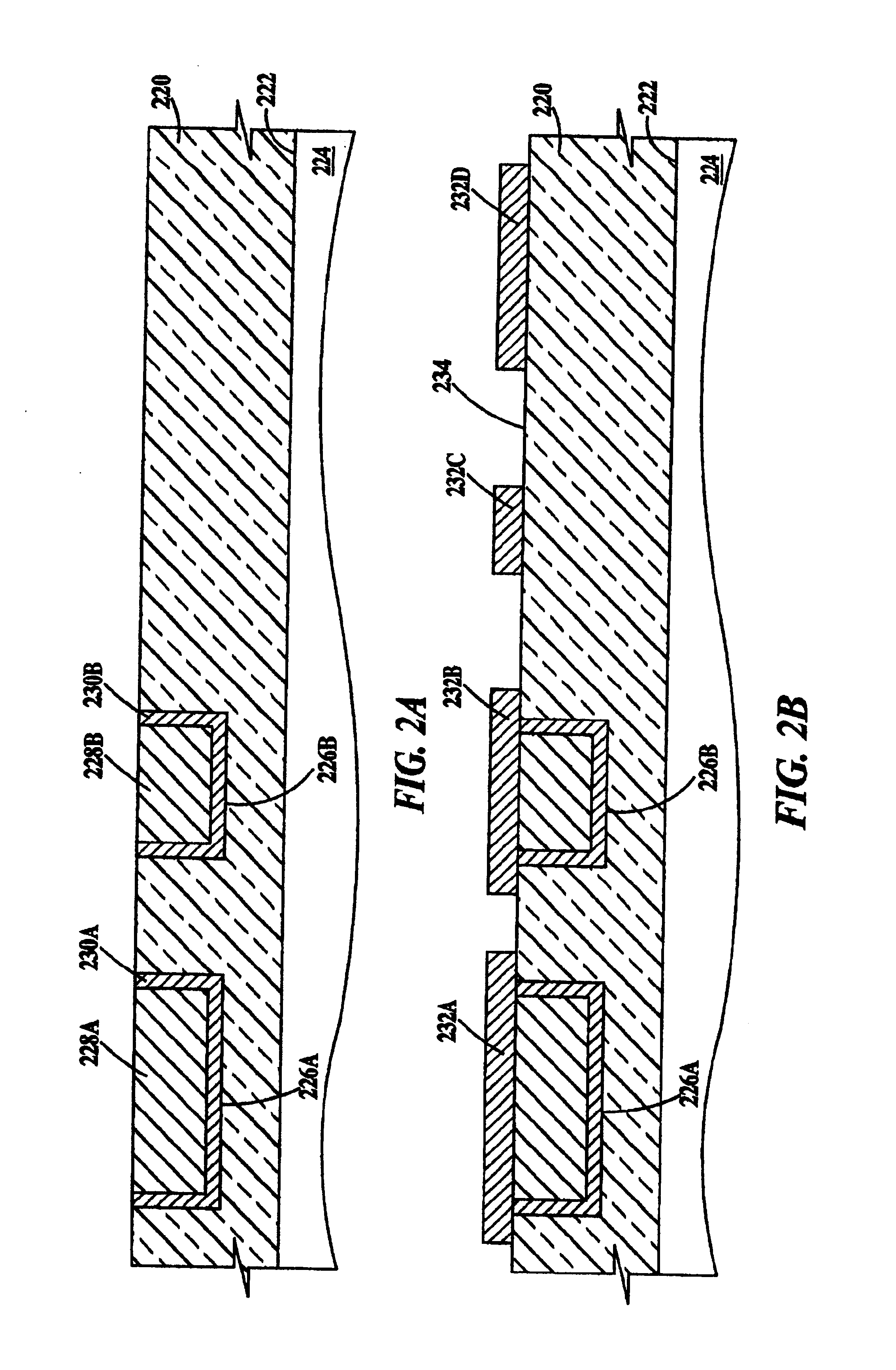
FIGS. 2A through 2F are cross-sectional views illustrating fabrication of a MIM capacitor according to the present invention. In FIG. 2A, an ILD 220 is formed on a top surface 222 of semiconductor substrate 224. Formed in ILD 220 are a bottom electrode 226A and a conductor 226B. Bottom electrode 226A includes a copper core conductor 228A and a conductive liner 230A. Conductor 226B includes a copper core conductor 228B and a conductive liner 230B. Conductive liner and ILD materials have been described supra. Bottom electrode 226A and conductor 226B are formed by a damascene process. In a damascene process, trenches are formed in an ILD by photo-lithographically patterning a masking layer applied over the ILD, performing a reactive ion etch (RIE) of the ILD, removing the masking layer, depositing a conductive liner, depositing a copper seed layer deposition, copper plating to fill the trench and performing a chemical-mechanical-polish (CMP) process to co-planarize the top surfaces of ...
second embodiment
FIGS. 4A through 4E are cross-sectional views illustrating fabrication of a MIM capacitor according to the present invention. In FIG. 4A, an ILD 320 is formed on a top surface 322 of semiconductor substrate 324. Formed in ILD 320 are a bottom electrode 326A and a conductor 328A. Bottom electrode 326A includes a copper core conductor 328A and a conductive liner 330A. Conductor 326B includes a copper core conductor 328B and a conductive liner 330B. Conductive liner and ILD materials have been described supra. Bottom electrode 326A and conductor 326B are formed by a damascene process as describes supra. Bottom electrode 326A will become the bottom electrode of a MIM capacitor and conductor 326B is a typical interconnect conductor.
In FIG. 4B, core conductors 328A and 328B are recessed by a wet process or an RIE process. A conductive diffusion barrier layer is deposited on ILD 320 of sufficient thickness to fill the recesses formed by the core etching process and a CMP process performed ...
third embodiment
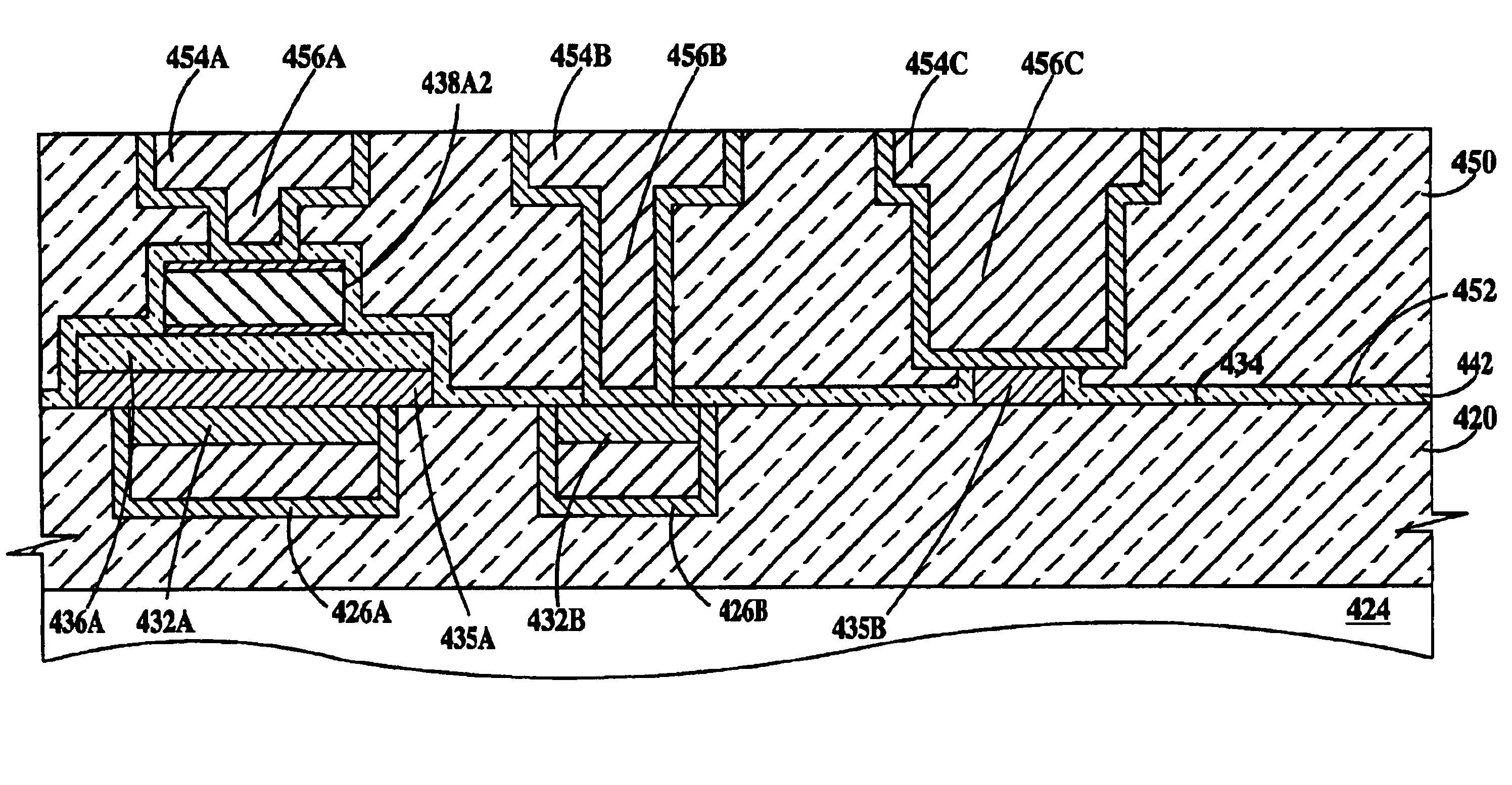
FIGS. 5A through 5F are cross-sectional views illustrating fabrication of a MIM capacitor according to the present invention. In FIG. 5A, an ILD 420 is formed on a top surface 422 of semiconductor substrate 424. Formed in ILD 420 are a bottom electrode 426A and a conductor 426B. Bottom electrode 426A includes a copper core conductor 428A and a conductive liner 430A. Conductor 426B includes a copper core conductor 428B and a conductive liner 430B. Conductive liner and ILD materials have been described supra. Bottom electrode 426A and conductor 426B are formed by a damascene process as describes supra. Bottom electrode 426A will become the bottom electrode of a MIM capacitor and conductor 426B is a typical interconnect conductor.
In FIG. 5B, core conductors 428A and 428B are recessed by a wet process or an RIE process. A first conductive diffusion barrier layer is deposited on ILD 420 of sufficient thickness to fill the recesses formed by the etch process and a CMP process performed to...
PUM
| Property | Measurement | Unit |
|---|---|---|
| thickness | aaaaa | aaaaa |
| thickness | aaaaa | aaaaa |
| thickness | aaaaa | aaaaa |
Abstract
Description
Claims
Application Information
 - R&D
- Intellectual Property
- Life Sciences
- Materials
- Tech Scout
- Unparalleled Data Quality
- Higher Quality Content
- 60% Fewer Hallucinations
Browse by: Latest US Patents, China's latest patents, Technical Efficacy Thesaurus, Application Domain, Technology Topic, Popular Technical Reports.
© 2025 PatSnap. All rights reserved.Legal|Privacy policy|Modern Slavery Act Transparency Statement|Sitemap|About US| Contact US: help@patsnap.com