

Apparatus and method for in-situ endpoint detection for chemical mechanical polishing operations
a technology of chemical mechanical polishing and apparatus, applied in the field of semiconductor/solid-state device testing/measurement, semiconductor machines, instruments, etc., can solve the problems of poor yield and device performance, high topography of in-process wafers, and uneven topography of the top surface of the wafers, etc., to achieve the effect of improving accuracy
- Summary
- Abstract
- Description
- Claims
- Application Information
AI Technical Summary
Benefits of technology
Problems solved by technology
Method used
Image

Examples
Embodiment Construction
Preferred embodiments of the present invention will now be described with reference to the drawings.
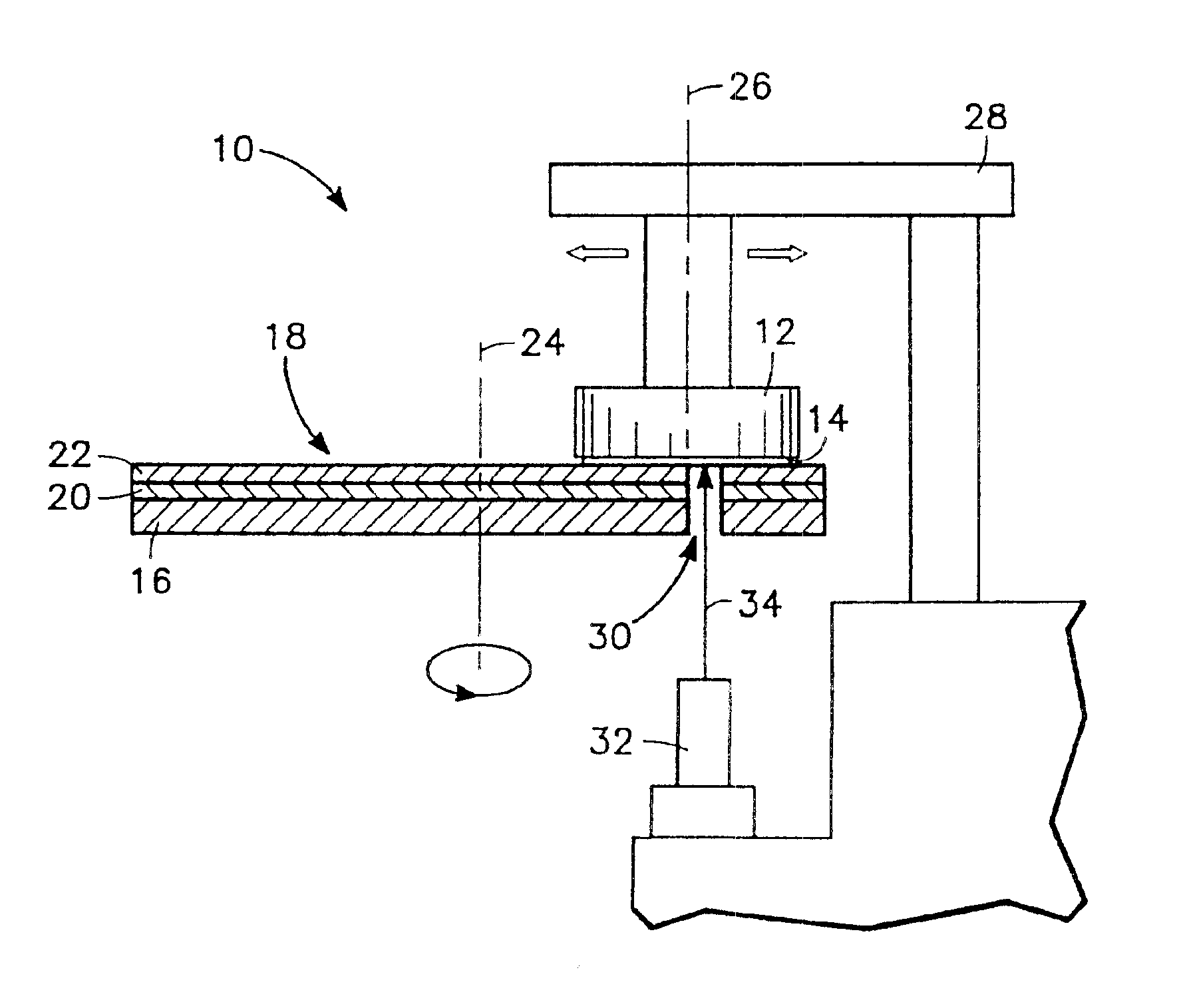
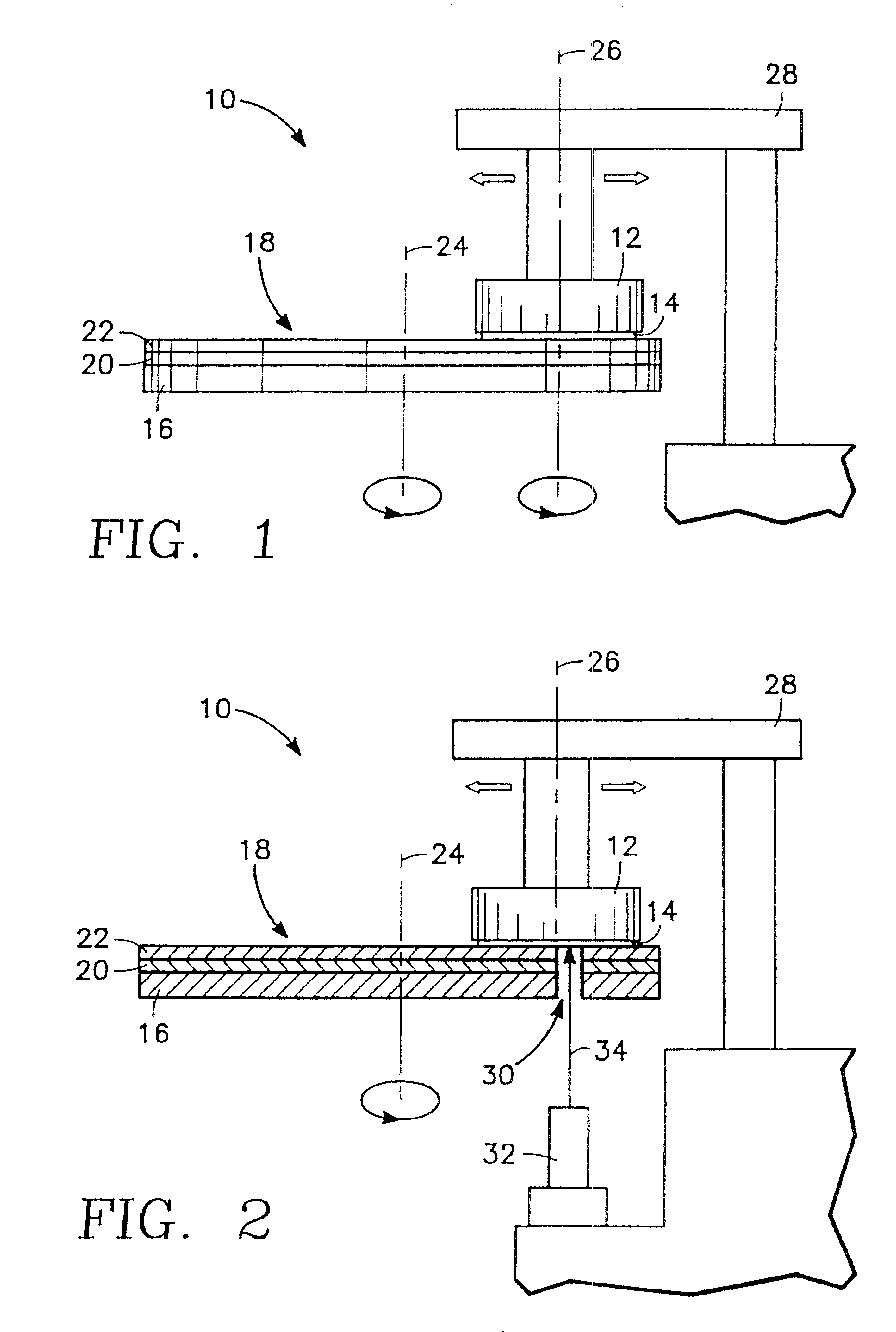
FIG. 2 depicts a portion of a CMP apparatus modified in accordance with one embodiment of the present invention. A hole 30 is formed in the platen 16 and the overlying platen pad 18. This hole 30 is positioned such that it has a view the wafer 14 held by a polishing head 12 during a portion of the platen's rotation, regardless of the translational position of the head 12. A laser interferometer 32 is fixed below the platen 16 in a position enabling a laser beam 34 projected by the laser interferometer 32 to pass through the hole 30 in the platen 16 and strike the surface of the overlying wafer 14 during a time when the hole 30 is adjacent the wafer 14.
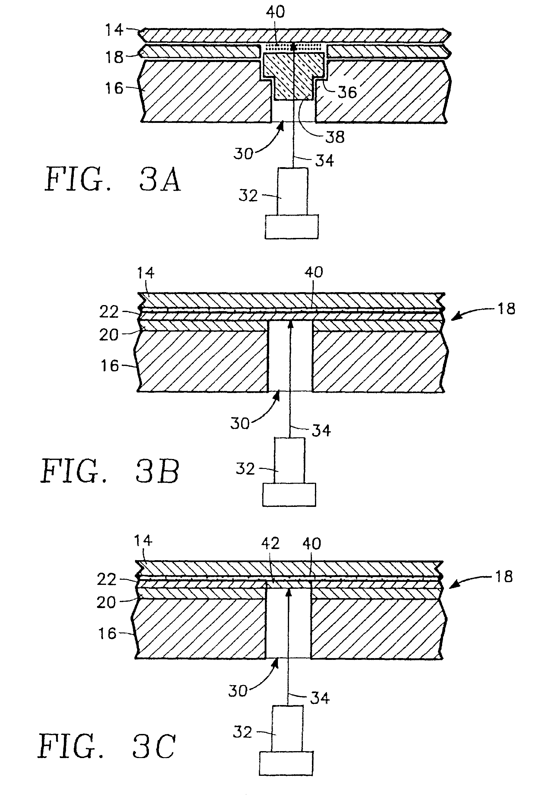
A detailed view of the platen hole Sand wafer 14 (at a time when it overlies the platen hole 30) are shown in FIGS. 3A-C. As can be seen in FIG. 3A, the platen hole 30 has a stepped diameter, thus forming a shoulder 36. The shoulder 36 i...
PUM
 Abstract
Description
Claims
Application Information