Method for improving ash rate uniformity in photoresist ashing process equipment

a technology of photoresist ashing and uniform ash rate, which is applied in the direction of ovens, lighting and heating apparatus, furniture, etc., can solve the problems of exhibiting an ash rate non-uniformity and reducing the photoresist removal rate from the edge to the center of the wafer

Inactive Publication Date: 2005-04-12
TEXAS INSTR INC
View PDF10 Cites 19 Cited by
  • Summary
  • Abstract
  • Description
  • Claims
  • Application Information

AI Technical Summary

Problems solved by technology

Certain types of equipment used in the ashing process for the removal of photoresist during the processing of integrated circuits and/or micro-electromechanical-mechanical (MEMS) devices, exhibit an ash rate non-uniformity from the edge-to-center of the wafer.
This effect, caused by a semi-stagnation of the plasma gas flow at the center of the wafer as compared to the

Method used


Image

  • Method for improving ash rate uniformity in photoresist ashing process equipment
  • Method for improving ash rate uniformity in photoresist ashing process equipment
  • Method for improving ash rate uniformity in photoresist ashing process equipment

Examples


first embodiment

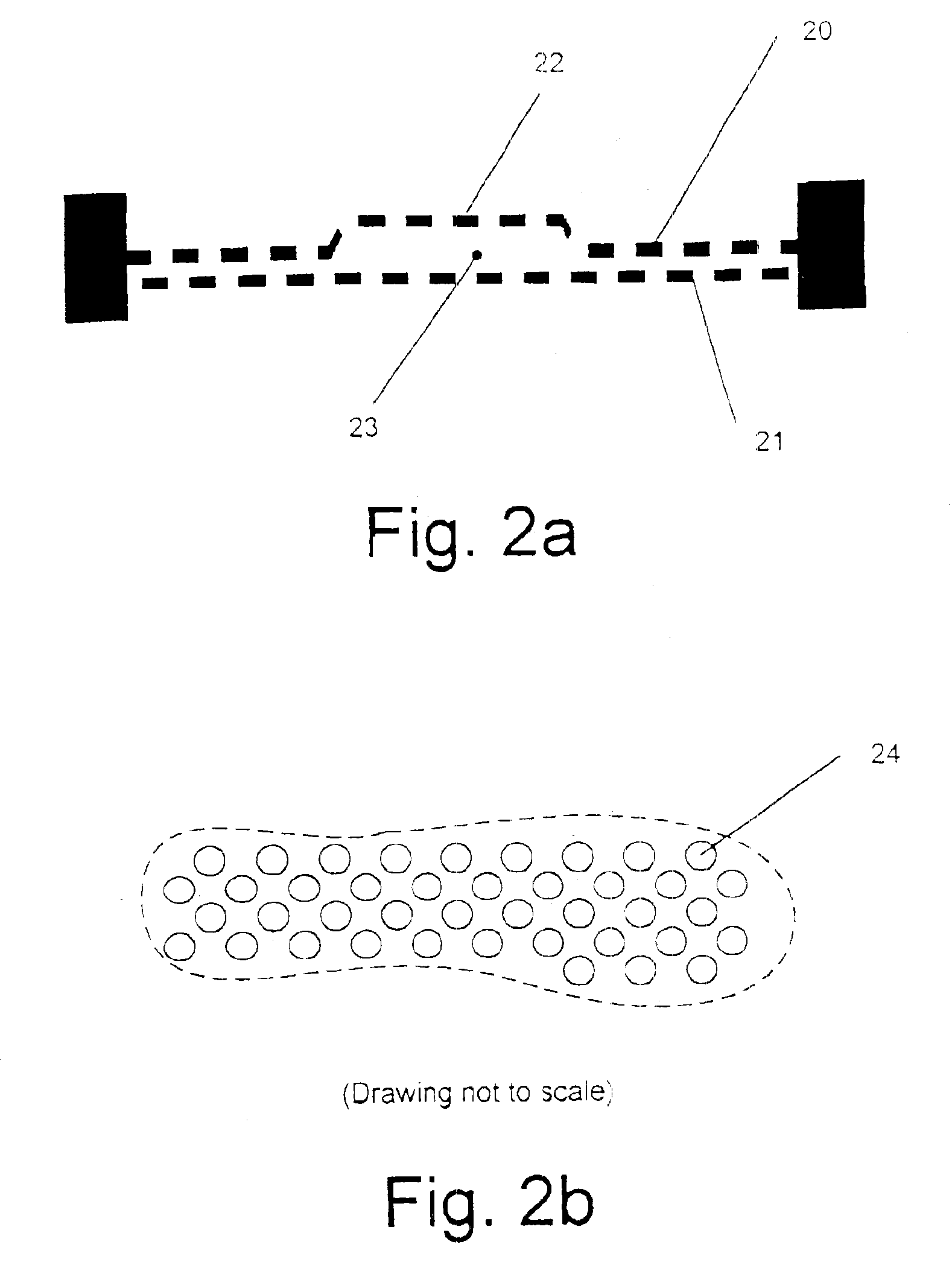
[0021]FIG. 2a shows the invention where the grid plate separation gap is made larger in a stepwise manner over the center region of the target wafer. The grid plates are comprised of an upper plate 20 and a lower plate 21 and are separated by a gap 23. In this case, a stepwise impression 22 is made in the center portion of the upper grid plate 20. This in turn, provides larger gap spacing 23 to be employed over the center of the target wafer. FIG. 2b shows the hole pattern 24, which maintains equal sized holes in the upper and lower grid plates 20 and 21, respectively. Gap spacing typically varies in the neighborhood of 0.035 to 0.050 inches. The wider gap near the center of the grid plates allows greater amounts of plasma gases to flow in this normally semi-stagnated area located around the center of the target wafer.

second embodiment

[0022]More accurate control of the ash rate uniformity is realized in this invention, as shown in FIGS. 3a and 3b. Here the gap 32 between upper grid plate 30 and lower grid plate 31 varies continuously from edge-to-center of the grid plate assembly. This eliminates the step function of embodiment one and provides more uniform plasma gas flow over the entire target wafer. As illustrated in FIG. 3b, the grid plate holes 33 are all of equal size. As before, the grid plate gap spacing varies in the range of 0.035 to 0.050 inches.

third embodiment

[0023]the invention is depicted in FIGS. 4a and 4b. In this case the grid plates 40 and 41 maintain a constant gap spacing 42, but the hole diameters 43 vary across the plates from edge-to-center, with the larger holes located near the center. The overall effect of this approach is the same as the earlier embodiments in that the plasma gas flow rate is increased in the semi-stagnation area near the center of the target wafer.

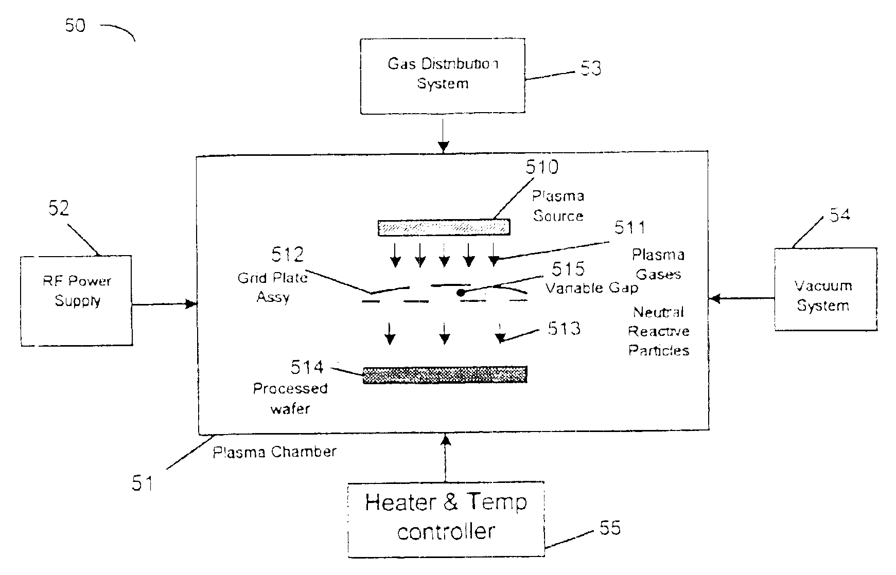
[0024]FIG. 5 is a block diagram for a plasma ashing machine 50, which uses the grid plate assembly 512 of this invention. This machine is comprised of a plasma chamber 51 with other necessary sources connected to the chamber, including a RF power supply 52, a gas distribution system 53, a vacuum system 54, and a heater and temperature controller 55. These sources are combined to control the environment inside the plasma chamber 51. The wafer 514 to be processed (work piece) is placed in the plasma chamber 51. Plasma gases 511 from the plasma source 510 are appli...


PUM

PropertyMeasurementUnit
Lengthaaaaaaaaaa
Fractionaaaaaaaaaa
Temperatureaaaaaaaaaa

Abstract

A method for improving the edge-to-center photoresist ash rate uniformity in lower temperature (typically, but not limited to <100° C.) processing of integrated circuits and micro-electro-mechanical devices. A varying gap distance 32 from the edge-to-center of the upper and lower grid plates, 30 and 31, of a plasma ashing machine is provided to allow additional flow of plasma gases into the normally semi-stagnated area near the center of the wafer being processed. This improvement overcomes the problem of slower photoresist removal in the center of the wafer. Three configurations of the invention is described, including both stepwise and continuous variation of the grid plate gap spacing and optionally, the variation of the size of grid plate holes in a parallel grid plate assembly.

Description

[0002]This application is a divisional and claims priority under 35 USC §119(e)(1) of application Ser. No. 09 / 746,100 filed Dec. 21, 2000 now U.S. Pat. No. 6,646,223, and provisional application No. 60 / 173,405 filed Dec. 28, 1999.BACKGROUND OF THE INVENTION[0003]1. Field of the Invention[0004]This invention relates to semiconductor processing equipment and more particularly to plasma ashing equipment.[0005]2. Description of the Related Art[0006]Certain types of equipment used in the ashing process for the removal of photoresist during the processing of integrated circuits and / or micro-electromechanical-mechanical (MEMS) devices, exhibit an ash rate non-uniformity from the edge-to-center of the wafer. This effect, caused by a semi-stagnation of the plasma gas flow at the center of the wafer as compared to the outer edge of the wafer, results in a decrease in the rate of photoresist removal from the edge to center of the wafer. In the past, this edge-to-center ash rate variation has b...

Claims


Application Information

Patent Timeline
IPC IPC(8): H01J37/32H01L21/302H01L21/3065
CPCH01J37/32431H01J2237/3342H01L21/3065
Inventor HOGAN, TIMOTHY J.TAYLOR, TIMOTHY A.
Owner TEXAS INSTR INC
Why Eureka
Try Eureka