
Triple-well charge pump stage with no threshold voltage back-bias effect

a charge pump and threshold voltage technology, applied in the direction of electric variable regulation, process and machine control, instruments, etc., can solve the problems of large back-bias voltage, large back-bias voltage, and significant efficiency loss, and achieve the effect of undetectable threshold voltages of associated transistors and large back-bias voltages

Inactive Publication Date: 2005-04-12
RPX CORP
View PDF30 Cites 72 Cited by
  • Summary
  • Abstract
  • Description
  • Claims
  • Application Information

AI Technical Summary

Benefits of technology

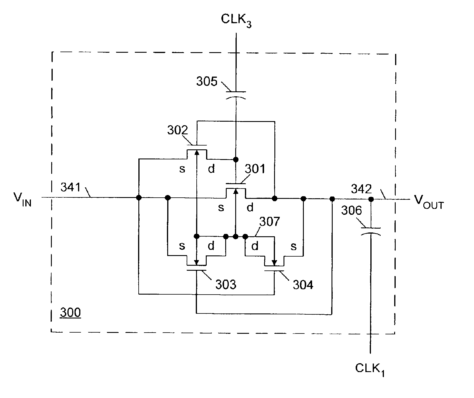
The third n-channel transistor couples the p-well to the input terminal when the output terminal is at a higher voltage than the input terminal (i.e., when the first capacitor is discharging). Similarly, the fourth n-channel transistor couples the p-well to the output terminal when the input terminal is at a higher voltage than the output terminal (i.e., when the first capacitor is charging). As a result, the p-well is always held at a voltage equal to the lower of the source voltage or the drain voltage of the first n-channel transistor. Thus, the source-to-body voltage of the first n-channel transistor is always zero. As a result, the charge pump stage of the present invention does not exhibit a threshold voltage increase due to the presence of a back bias voltage. Consequently, the charge pump stage of the present invention can efficiently provide a boosted output voltage at the output terminal, even if numerous charge pump stages are connected in series. Moreover, by controlling the p-well voltage in the above-described manner, the charge pump stage of the present invention advantageously limits the gate-to-bulk voltage of the first n-channel transistor.

Problems solved by technology

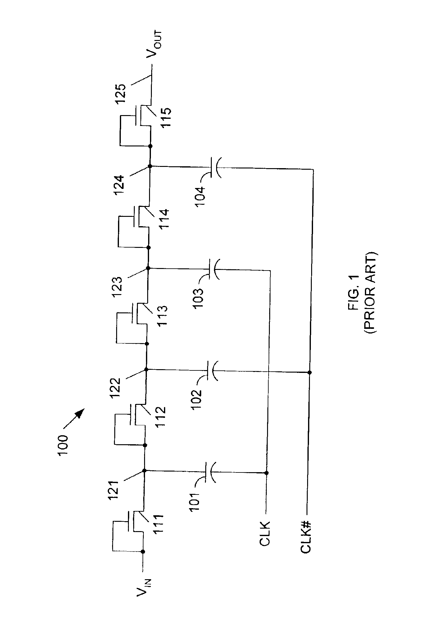
Implementing charge pump 100 using conventional CMOS circuitry results in two drawbacks related to the voltage drop on each of diode-connected NMOS transistors 111-115.
First, the threshold voltage loss on each of the diode-connected NMOS transistors 111-115 causes significant efficiency losses, especially at high output voltage levels where these transistors 111-115 are susceptible to large back-bias voltages.
Large back-bias voltages undesirably increase the threshold voltages of the associated transistors.
Second, the gate-to-bulk voltages VGB of the diode-connected transistors closer to output terminal 125 become undesirably large, thereby resulting in gate oxide stress within these transistors.
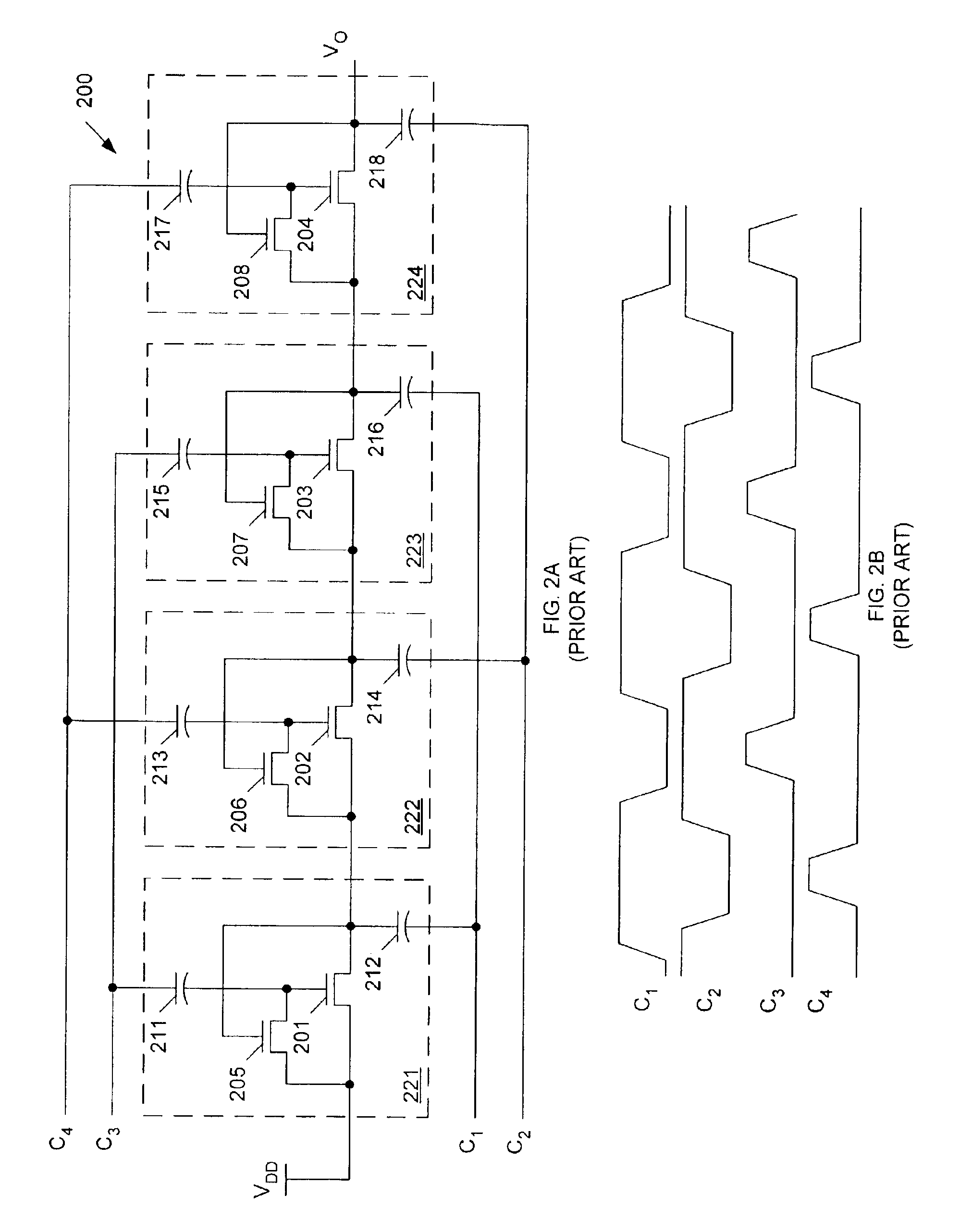
Moreover, the gate-to-bulk voltages VGB of the transistors 204 and 208 in the last output stage 224 become undesirably large, thereby resulting in gate oxide stress within these transistors.

Method used


Image

  • Triple-well charge pump stage with no threshold voltage back-bias effect
  • Triple-well charge pump stage with no threshold voltage back-bias effect
  • Triple-well charge pump stage with no threshold voltage back-bias effect

Examples


Embodiment Construction

FIG. 3 is a circuit diagram of a charge pump stage 300 in accordance with one embodiment of the present invention. Charge pump stage 300 includes n-channel MOS transistors 301-304, capacitors 305-306, input terminal 341 and output terminal 342. N-channel transistors 301-304 are fabricated in a p-well region 307. In the described embodiment, charge pump stage 300 is fabricated using a triple well process, wherein p-well region 307 is fabricated in a surrounding n-well region (not shown). The n-well region is located in a p-type substrate (not shown).

Because a triple-well process is typically used to fabricate EEPROM cells, charge pump stage 300 can be fabricated on the same chip as EEPROM cells without requiring process modifications. Charge pump stage 300 can then be used to generate the voltages required to operate the EEPROM cells.

N-channel transistor 301 is connected in series between input terminal 341 and output terminal 342. More specifically, the source of n-channel transisto...


PUM


Abstract

A charge pump stage includes a first n-channel transistor having a source coupled to an input terminal and a drain coupled to an output terminal. A second n-channel transistor has a source coupled to the input terminal, a drain coupled to a gate of the first transistor, and a gate coupled to the output terminal. A third n-channel transistor has a source coupled to the input terminal, a gate coupled to the output terminal, and a drain coupled to a p-well. A fourth n-channel transistor has a source coupled to the output terminal, a gate coupled to the input terminal, and a drain coupled to the p-well. The first, second, third and fourth transistors are fabricated in the p-well, which is surrounded by an n-well. A first capacitor is coupled to the output terminal, and a second capacitor is coupled to the gate of the first transistor.

Description

FIELD OF THE INVENTIONThe present invention relates to a charge pump circuit for generating a voltage on an integrated circuit device. More specifically, the present invention relates to a charge pump circuit having no back-bias effect.RELATED ARTElectrically erasable and programmable read only memory (EEPROM) devices require various voltages for their operation. For example, microflash SONOS type memory of the type described in U.S. Pat. No. 5,768,192, to Eitan requires a 9 Volt gate voltage for programming, a 4 Volt gate voltage for reading and a −6 Volt gate voltage for erasing. All these voltages are generated internally (i.e., inside the chip) in response to a VDD supply voltage by a charge pump circuit.FIG. 1 is a circuit diagram of a conventional charge pump circuit 100, introduced by J. Dickson, “On-Chip, High-Voltage Generation in NMOS Integrated Circuits Using an Improved Voltage Multiplier Technique”, Journal of Solid-State Circuits, Vol. SC-11, No. 3, pp. 374-378, June 1...

Claims


Application Information

Patent Timeline
Patent Type & Authority Patents(United States)
IPC IPC(8): H01L27/108G11C5/14H02M3/07H10B12/00
CPCG11C5/145H02M3/073H02M2003/078H02M2003/075H02M3/075H02M3/078
Inventor ESHEL, NOAM
Owner RPX CORP
Learn More