Non-volatile flash memory having a specific difference between source/floating gate and drain/floating gate overlapped portions

a non-volatile flash memory and overlapped portion technology, applied in the direction of semiconductors, electrical devices, transistors, etc., can solve the problems of slow data writing speed, inability to suppress punch-through current by this method, and inability to reduce the area of the array, so as to reduce the area of the memory cell

Inactive Publication Date: 2005-04-12
RENESAS ELECTRONICS CORP
View PDF7 Cites 1 Cited by
  • Summary
  • Abstract
  • Description
  • Claims
  • Application Information

AI Technical Summary

Benefits of technology

It is therefore an object of the present invention to provide a structure of a non-volatile flash memory manufacturing by micro processes, in which the generation of a punch-through current is suppressed and a common source line structure being capable of reducing a memory cell area can be also used, and a method in which data writing to an unselected memory cell is effectively prevented by using this structure.

Problems solved by technology

Consequently, there is a problem that the data writing speed is made to be slow.
However, under the situation that the semiconductor device has been manufacture by the further micro processes, it has been impossible that the punch-through current is suppressed by this method.
However, at the conventional method in which the same voltage is applied to the source 3 and the drain 4 at the data writing, the common source line structure can not be used, therefore the punch-through current can be suppressed, but there is a problem that the area of the array can not be reduced.

Method used


Image

  • Non-volatile flash memory having a specific difference between source/floating gate and drain/floating gate overlapped portions
  • Non-volatile flash memory having a specific difference between source/floating gate and drain/floating gate overlapped portions
  • Non-volatile flash memory having a specific difference between source/floating gate and drain/floating gate overlapped portions

Examples


first embodiment

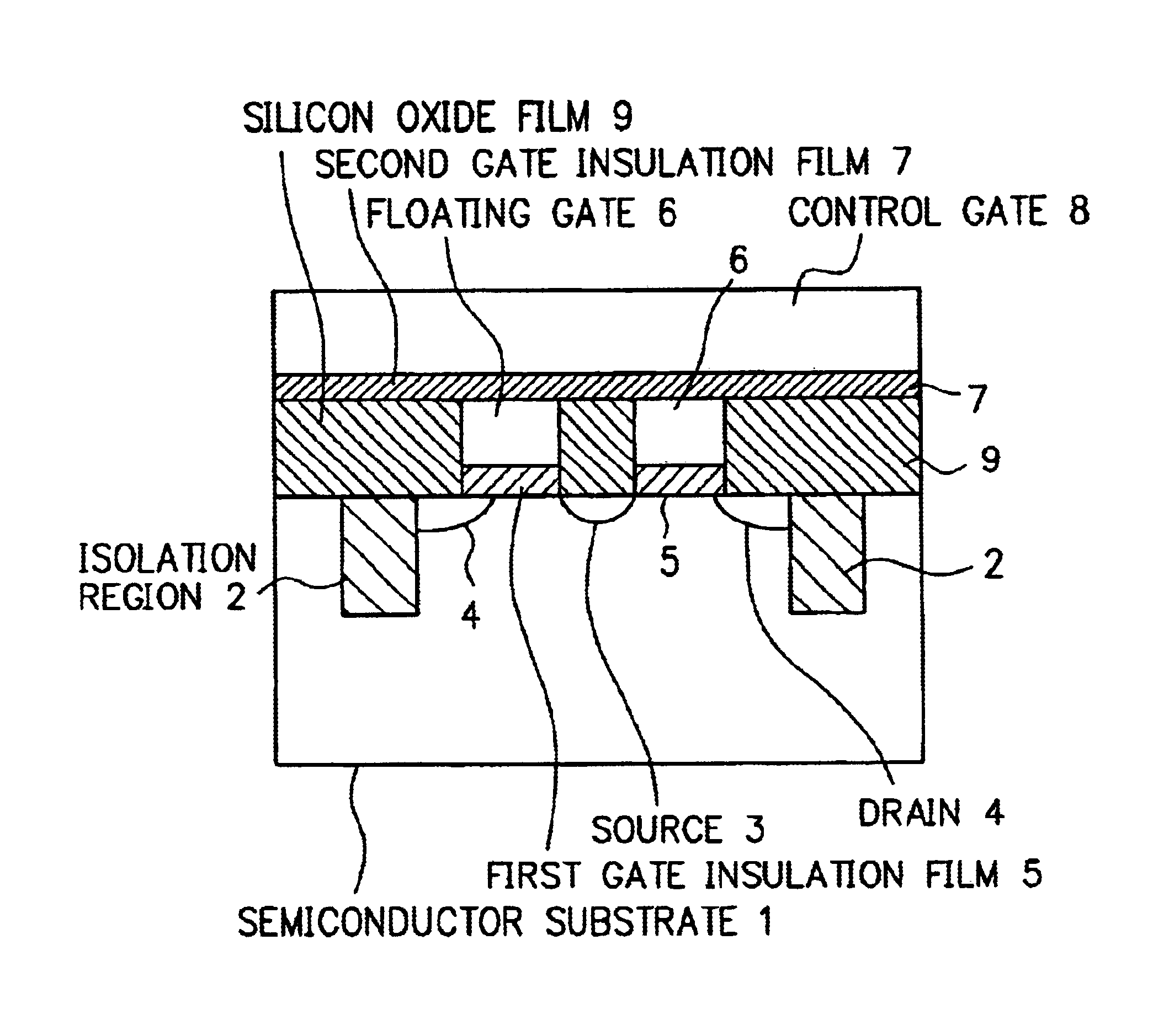
FIG. 4 is a sectional view at the A—A line of FIG. 3 of the structure of the non-volatile flash memory of the present invention. As shown in FIG. 4, the isolation regions 2, the source 3, and the drains 4 are formed on the surface of a semiconductor substrate 1. And on the surface of the semiconductor substrate 1 between the source 3 and one of the drains 4, a first gate insulation film 5 being a tunnel film, a floating gate 6, a second gate insulation film 7 being an inter poly silicon film, and the control gate 8 are formed in order from the bottom. And at the both sides of the floating gate 6 and the first gate insulation film 5 in the sectional view, a silicon oxide film 9 is formed. And there is a large overlapped region between the floating gate 6 and one of the drains 4 through a part of the first gate insulation film 5 being the tunnel film. And an overlapped region between the source 3 and the floating gate 6 is small. And at the position between the source 3 and the other ...

third embodiment

As mentioned above, at the third embodiment, since the impurity concentration of the first sources 30 are low, overlapped regions are not formed between the first sources 30 and the floating gates 6. And further, the second source 31 whose impurity concentration is high exists, therefore, there is an effect that the source resistance becoming high does not occur.

According to the structure of the non-volatile flash memory of the present invention, at a NOR type flash memory having a common source line, a region overlapped a drain and a floating gate of a memory cell is made to be large, and a region overlapped a source and the floating gate is made to be small. Therefore, at the time when data are written in the memory cell, a negative voltage is applied to a selected ward line (control gate), and the same value of a positive voltage is applied to a selected bit line (drain) and a common source line. With this, electrons can be ejected from the floating gate to the drain, without a p...


PUM


Abstract

A structure of a non-volatile flash memory, in which a punch-through current is suppressed and the area of a memory cell is reduced, is provided. The non-volatile flash memory being a NOR type non-volatile flash memory provides floating gates and a common source line, and drains. And at the structure of the non-volatile flash memory, a region overlapped one of the drains and one of the floating gates in a memory cell is larger than a region overlapped the common source and one of the floating gates in the memory cell.

Description

BACKGROUND OF THE INVENTIONThe present invention relates to a structure and a manufacturing method of a non-volatile flash memory.DESCRIPTION OF THE RELATED ARTAs one of the data writing operation to a non-volatile flash memory, there is a method ejecting electrons from a region overlapped a floating gate and a drain by using a Fauler-Nordheim (FN) type tunneling.Referring to drawings, this electron ejecting operation is explained. FIG. 1 is a sectional view at the A—A line of FIG. 2 of a structure of a conventional non-volatile flash memory. As shown in FIG. 1, at the conventional non-volatile flash memory, isolation regions 2, a source 3, and a drain 4 are formed on a semiconductor substrate 1. And on the surface of the semiconductor substrate 1 between the source 3 and the drain 4, a first gate insulation film 5 being a tunnel film, a floating gate 6, a second gate insulation film 7 being an inter poly silicon film, and a control gate 8 are formed in order from the bottom. And a ...

Claims


Application Information

Patent Timeline
Patent Type & Authority Patents(United States)
IPC IPC(8): H01L21/70H01L27/115H01L21/44H01L29/66H01L21/02H01L21/336H01L21/8247H01L29/788H01L29/792
CPCH01L27/11521H01L27/115H10B69/00H10B41/30
Inventor TSUKIJI, MASARU
Owner RENESAS ELECTRONICS CORP
Why Eureka
Try Eureka