High output nonvolatile magnetic memory

a nonvolatile, magnetic memory technology, applied in the direction of magnets, instruments, substrates/intermediate layers, etc., can solve the problems of large amount of power, low output, and reversal of magnetization, so as to reduce the number of electrode wires, reduce the power required, and increase the output of the tmr device

Inactive Publication Date: 2005-01-11
HITACHI LTD
View PDF3 Cites 94 Cited by
  • Summary
  • Abstract
  • Description
  • Claims
  • Application Information

AI Technical Summary

Benefits of technology

A first objective is to decrease the number of electrode wires.
A second objective is to reduce the power required to reverse magnetization of a free layer in the TMR device independent of a current induced magnetic field.
A third objective is to increase output of the TMR device.
It is possible to provide magnetization reversal independent of switching and a current induced magnetic field by installing the above-mentioned two-terminal nonvolatile magnetic memory cell in the magnetic memory. Thus, it is possible to decrease a memory cell area and provide a large-scale integration.

Problems solved by technology

Unfortunately, the conventional CMOS has a multitude of electrode wires.
Unfortunately, a very large amount of power is needed to induce a magnetic field enough to cause the magnetization reversal.
Unfortunately, such an output is relatively low.

Method used


Image

  • High output nonvolatile magnetic memory
  • High output nonvolatile magnetic memory
  • High output nonvolatile magnetic memory

Examples


embodiment 1

[Embodiment 1]

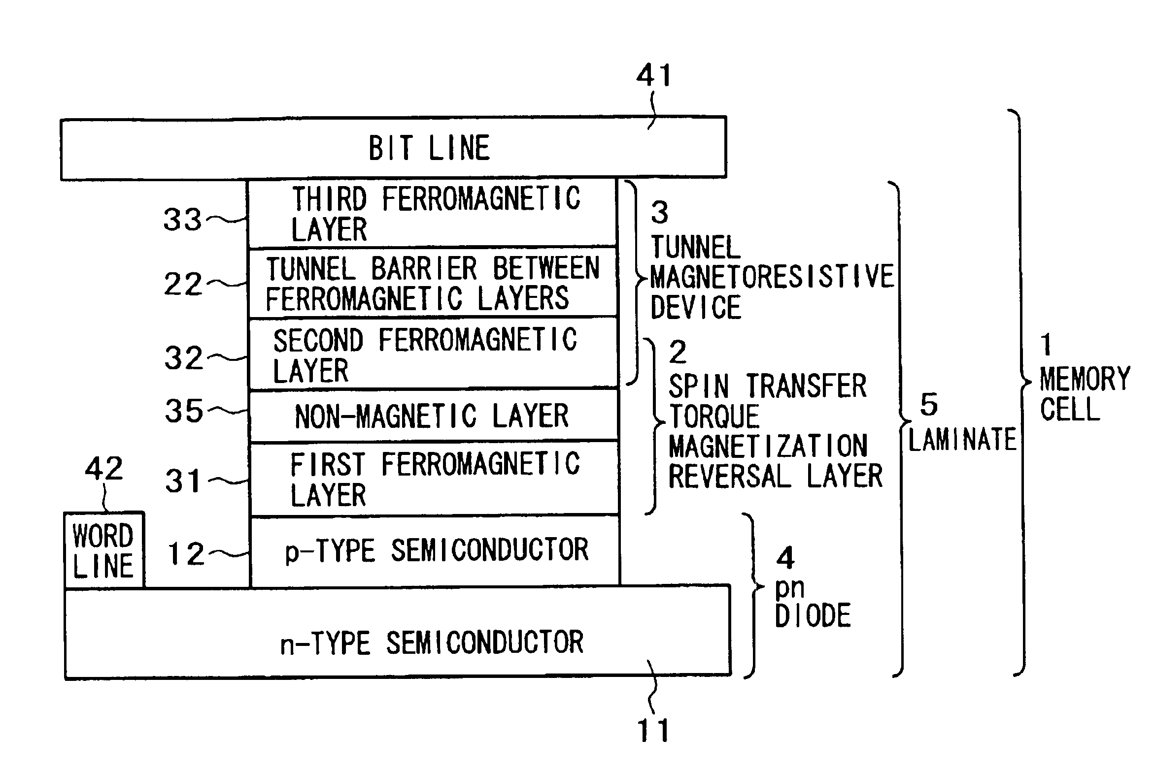
FIG. 1 schematically shows a sectional view of one memory cell according to the embodiment. A p-type semiconductor 12 is arranged on an n-type semiconductor 11 to form a pn junction. The pn junction comprises n-GaAs as an n-type semiconductor and p-GaAs as a p-type semiconductor. It may be preferable to use InGaAs for these semiconductors. The molecular beam epitaxy (MBE) is used to form the semiconductors.

Then, sputtering is used to form Co as a first ferromagnetic layer 31 and Cu as a non magnetic layer 35 without exposure from an ultra-high vacuum atmosphere. A laminated layer of the first ferromagnetic layer 31 and the non magnetic layer 35 is used to fabricate a spin transfer torque magnetization reversal layer 2. Then, a second ferromagnetic layer 32 of CoFe is formed, and a tunnel barrier between ferromagnetic layers 22 as Al is formed in this order.

Thereafter, plasma oxidation is applied to Al on the top surface without breaking the ultra-high vacuum atmosphere...

embodiment 2

[Embodiment 2]

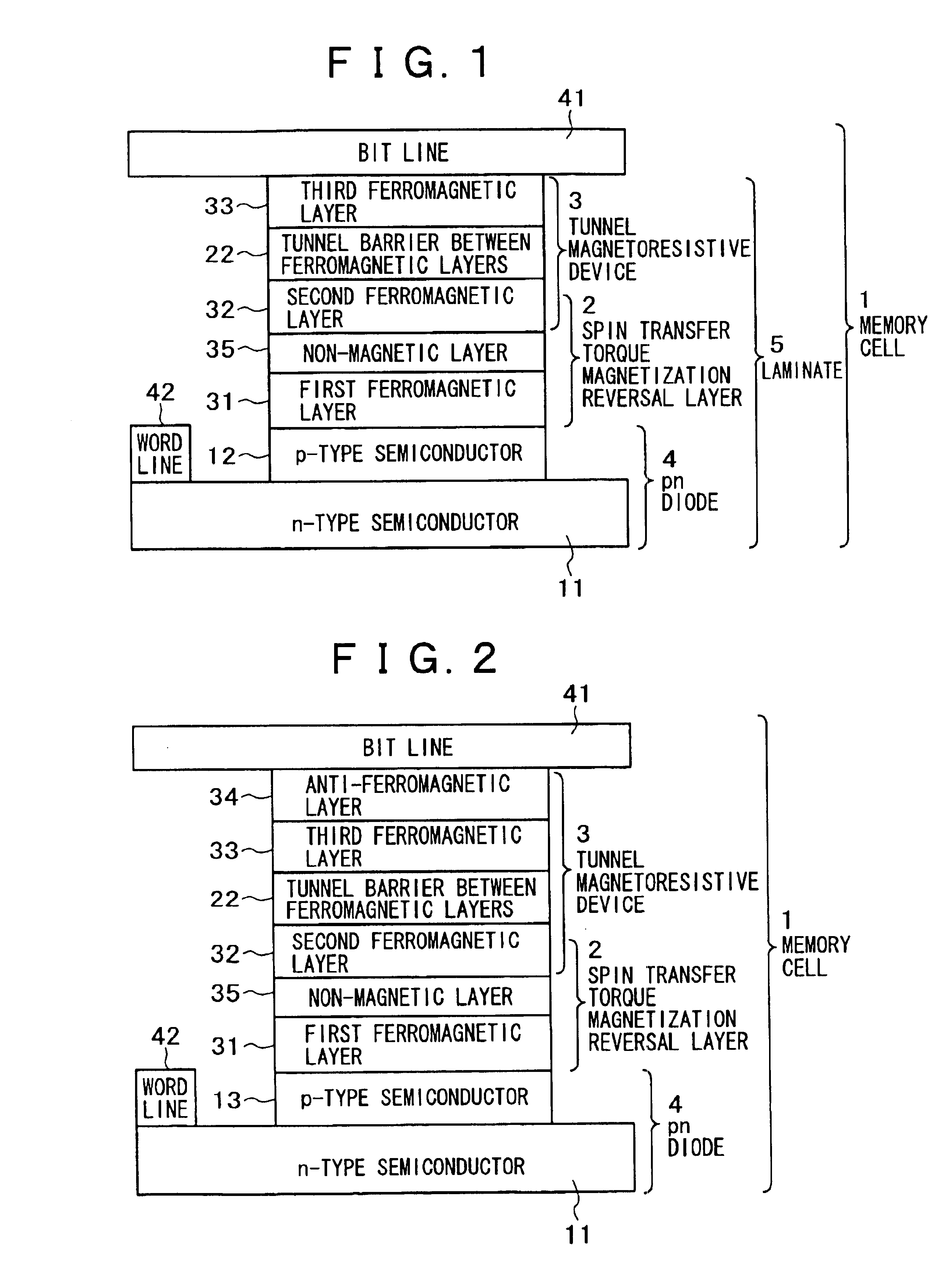
FIG. 2 schematically shows a sectional view of a memory cell having an anti-ferromagnetic layer 34 in order to fix the magnetization direction of the third ferromagnetic layer according to the configuration in FIG. 1. The antiferromagnetic layer 34 uses MnPt. The other layer configurations of the memory cell 1 are the same as for the embodiment 1. Like the embodiment 1, photo lithography and EB lithography are used to form cells.

Like the embodiment 1, the embodiment 2 can use a current to arrange the magnetization direction of the second ferromagnetic free layer 32 parallel or anti-parallel to the magnetization direction of the third ferromagnetic layer 33, allowing magnetization reversal independent of a current-induced magnetic field. The manufactured cell also yielded representative current-voltage characteristics as shown in FIG. 13.

embodiment 3

[Embodiment 3]

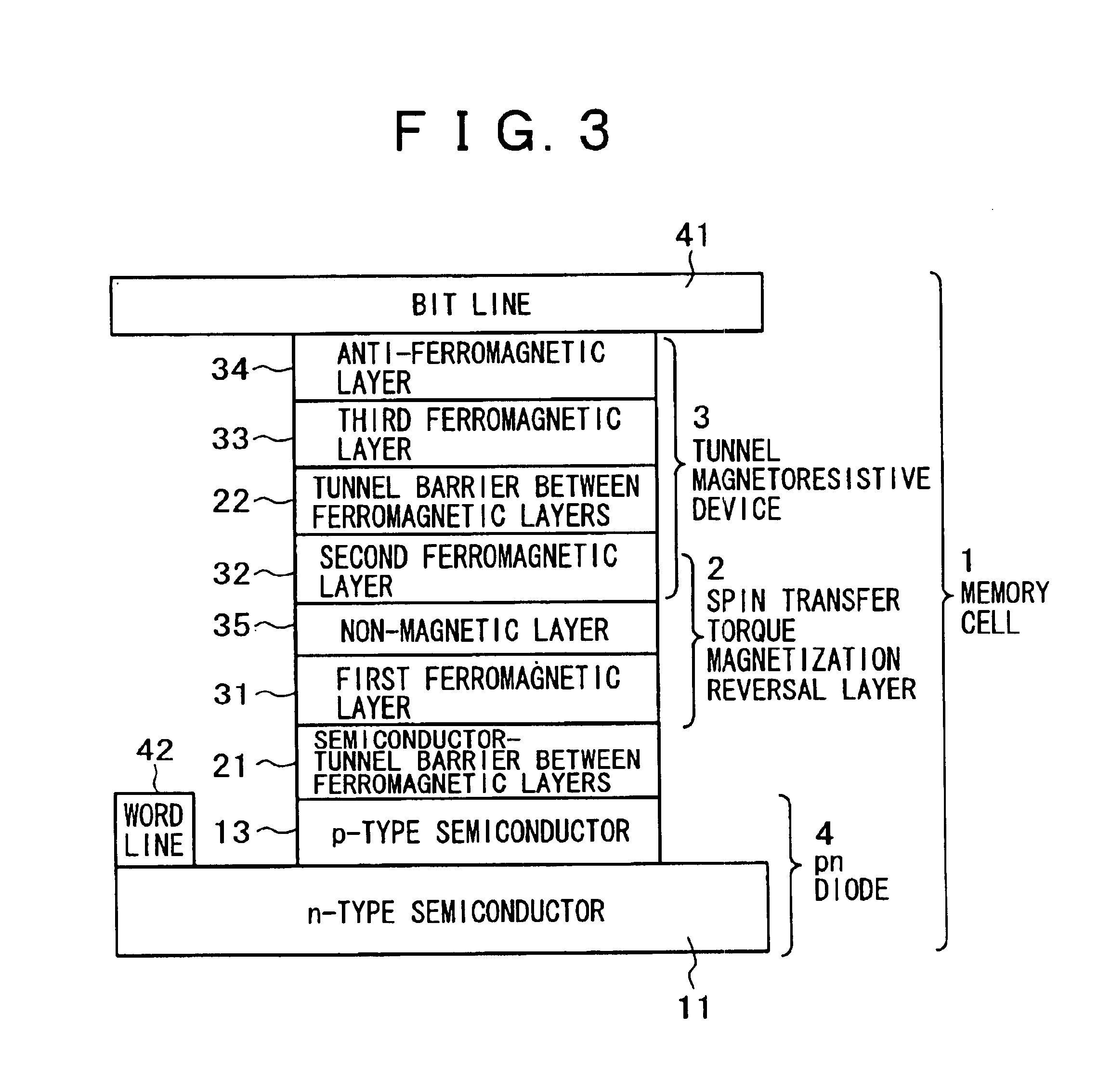
FIG. 3 schematically shows a sectional view of a memory cell that forms a tunnel barrier between semiconductor and ferromagnetic layer between the pn diode and the first ferromagnetic layer according to the configuration in FIG. 2. This tunnel barrier between diode and ferromagnetic layer uses AlAs. The other layer configurations of the memory cell 1 are the same as for the embodiment 2. Like the embodiment 2, the embodiment 3 uses photo lithography, etching, and EB lithography to form cells.

Like the embodiment 1, the embodiment 3 can use a current to arrange the magnetization direction of the second ferromagnetic free layer 32 parallel or anti-parallel to the magnetization direction of the third ferromagnetic layer 33, allowing magnetization reversal independent of a current-induced magnetic field.

The manufactured cell also yielded representative current-voltage characteristics as shown in FIG. 13.


PUM

PropertyMeasurementUnit
magnetoresistiveaaaaaaaaaa
nonmagneticaaaaaaaaaa
spin currentaaaaaaaaaa

Abstract

A magnetic memory is provided with a high-output memory cell capable of switching and magnetization reversal operations by means of two terminals. There is formed an MIS junction laminated layer comprising a diode, a spin transfer torque magnetization reversal induction layer, and a tunnel magnetoresistive device. A bit line and a word line are connected to the laminated layer.

Description

COPYRIGHT NOTICEA portion of the disclosure of this patent document contains material which is subject to copyright protection. The copyright owner has no objection to the facsimile reproduction by anyone of the patent document or the patent disclosure, as it appears in the Patent and Trademark Office patent file or records, but otherwise reserves all copyright rights whatsoever.BACKGROUND OF THE INVENTION1. Field of the InventionThe present invention generally relates to nonvolatile magnetic memories and, more particularly, to high-output nonvolatile magnetic memories having switching and spin torque magnetization reversal capabilities.2. Discussion of BackgroundAs shown in FIG. 14, conventional nonvolatile magnetic memory comprises a cell by forming a tunnel magnetoresistive (TMR) device on a complimentary metal-oxide semiconductor field-effect transistor (CMOSFET). The complimentary metal-oxide semiconductor (CMOS) is used for switching. A TMR device (e.g., see non-patent documen...

Claims


Application Information

Patent Timeline
Patent Type & Authority Patents(United States)
IPC IPC(8): G11C11/15G11C11/02H01F10/16H01F10/32H01L21/8246H01L27/105H01L43/08H01L43/10
CPCB82Y25/00G11C11/15H01F10/329H01F10/3254G11C11/16H01F10/3272
Inventor HAYAKAWA, JUN
Owner HITACHI LTD
Why Eureka
Try Eureka