Semiconductor memory device with memory cell having low cell ratio

a memory cell and semiconductor technology, applied in semiconductor devices, digital storage, instruments, etc., can solve the problems of data not being written, data being destroyed, impedance when the driver transistor is conductive too low, etc., to reduce the area of the memory cell, reduce the quantity of charges, and ensure the capacity value of the storage node included in the memory cell.

Inactive Publication Date: 2005-02-22
RENESAS ELECTRONICS CORP
View PDF5 Cites 9 Cited by
  • Summary
  • Abstract
  • Description
  • Claims
  • Application Information

AI Technical Summary

Benefits of technology

By the semiconductor memory device according to the present invention, the capacitance value of a storage node included in a memory cell is assured, a memory cell has the ratioless configuration, and the quantity of charges supplied from a bit line pair to a storage node at the time of reading / writing data is sufficiently assured. Thus, the area of the memory cell is reduced, thereby realizing higher packing density, and stable and high-speed operation with a low voltage is realized.

Problems solved by technology

Therefore, when the other driver transistor is turned on, the stored data is destroyed.
However, when the current drivability of the driver transistor is increased too much, impedance when the driver transistor is conductive becomes too low and a problem such that data cannot be written occurs.
On the contrary, when the current drivability of the driver transistor is lowered so that data is easily written, as described above, stored data is destroyed at the time of reading operation.
However, the reading operation in the SRAM is destructive reading that data stored in a memory cell is once destroyed.
Consequently, in the SRAM, further increase in processing speed and further reduction in power consumption cannot be realized.
Although it can be considered to decrease the threshold voltage of the transistor, if the threshold voltage is decreased, a leak current in an OFF state increases and power consumption in a standby mode increases.
Therefore, a conventional SRAM cannot sufficiently deal with lower power consumption.
Consequently, time required for the writing operation increases by the amount.
As the voltage is decreasing, time required for charging / discharging the capacity increases, so that it becomes difficult to realize higher processing speed of the semiconductor memory device.

Method used


Image

  • Semiconductor memory device with memory cell having low cell ratio
  • Semiconductor memory device with memory cell having low cell ratio
  • Semiconductor memory device with memory cell having low cell ratio

Examples


first embodiment

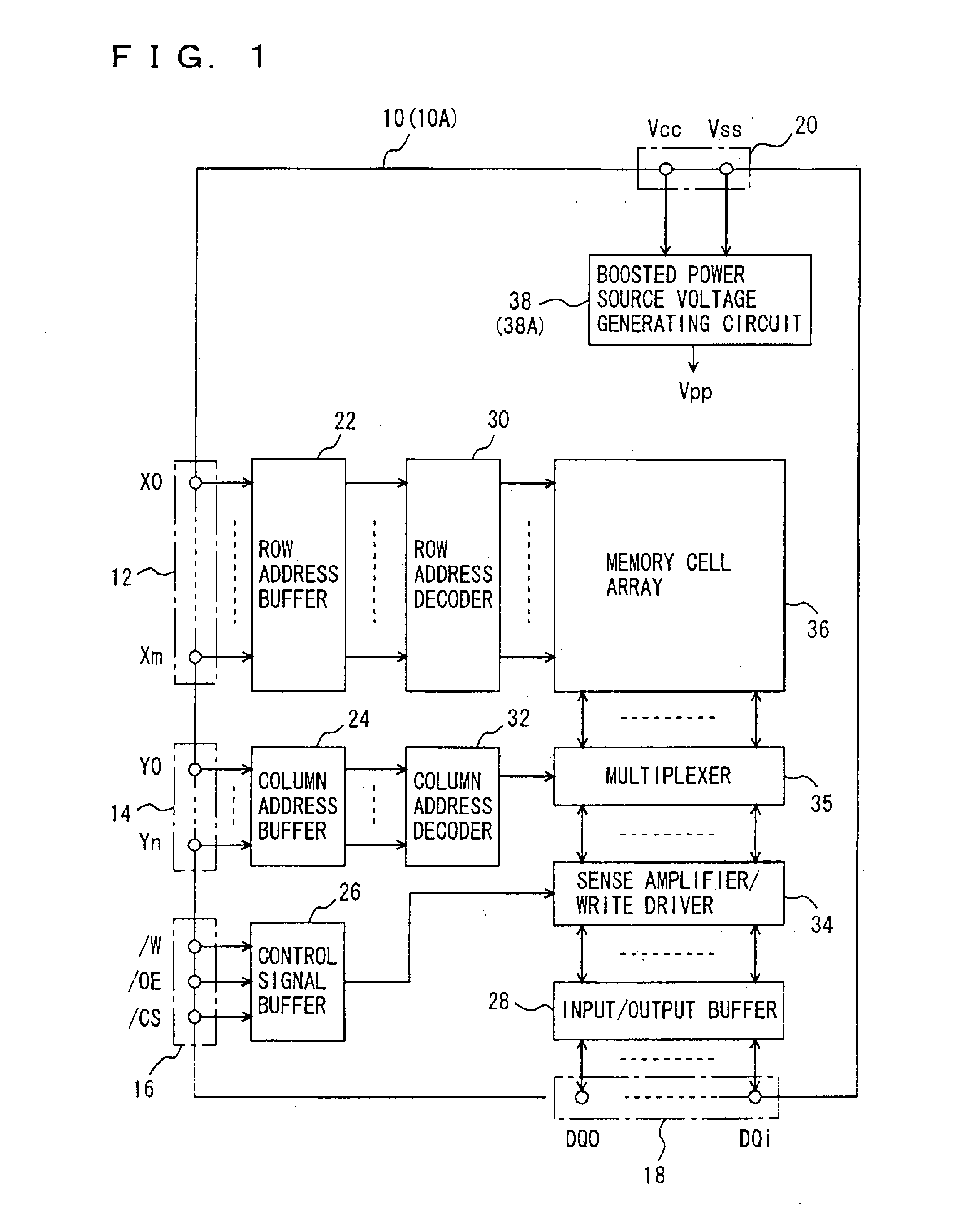
FIG. 1 is a general block diagram conceptually showing the configuration of a semiconductor memory device 10 according to a first embodiment of the present invention.

Referring to FIG. 1, semiconductor memory device 10 has a row address terminal 12, a column address terminal 14, a control signal terminal 16, a data input / output terminal 18, and a power source terminal 20. Semiconductor memory device 10 also has a row address buffer 22, a column address buffer 24, a control signal buffer 26, and an input / output buffer 28. Further, semiconductor memory device 10 has a row address decoder 30, a column address decoder 32, a sense amplifier / write driver 34, a multiplexer 35, a memory cell array 36, and a boosted power source voltage generating circuit 38.

Row address terminal 12 and column address terminal 14 receive row address signals X0 to Xm and column address signals Y0 to Yn (m and n: natural numbers), respectively. Control signal terminal 16 receives a write control signal / W, an out...

second embodiment

In a second embodiment, a bit line precharge circuit is constructed by N-channel MOS transistors.

Referring again to FIG. 1, a semiconductor memory device 10A according to a second embodiment has a configuration similar to that of semiconductor memory device 10 according to the first embodiment except that a boosted power source voltage generating circuit 38A is provided in place of boosted power source voltage generating circuit 38. Boosted power source voltage generating circuit 38A is different from boosted power source voltage generating circuit 38 with respect to the points that it outputs generated voltage Vpp to a word line driver included in row address decoder 30 and also to a not-shown BLPC signal generating circuit.

Since the other configuration of semiconductor memory device 10A is the same as that of semiconductor memory device 10, its description will not be repeated.

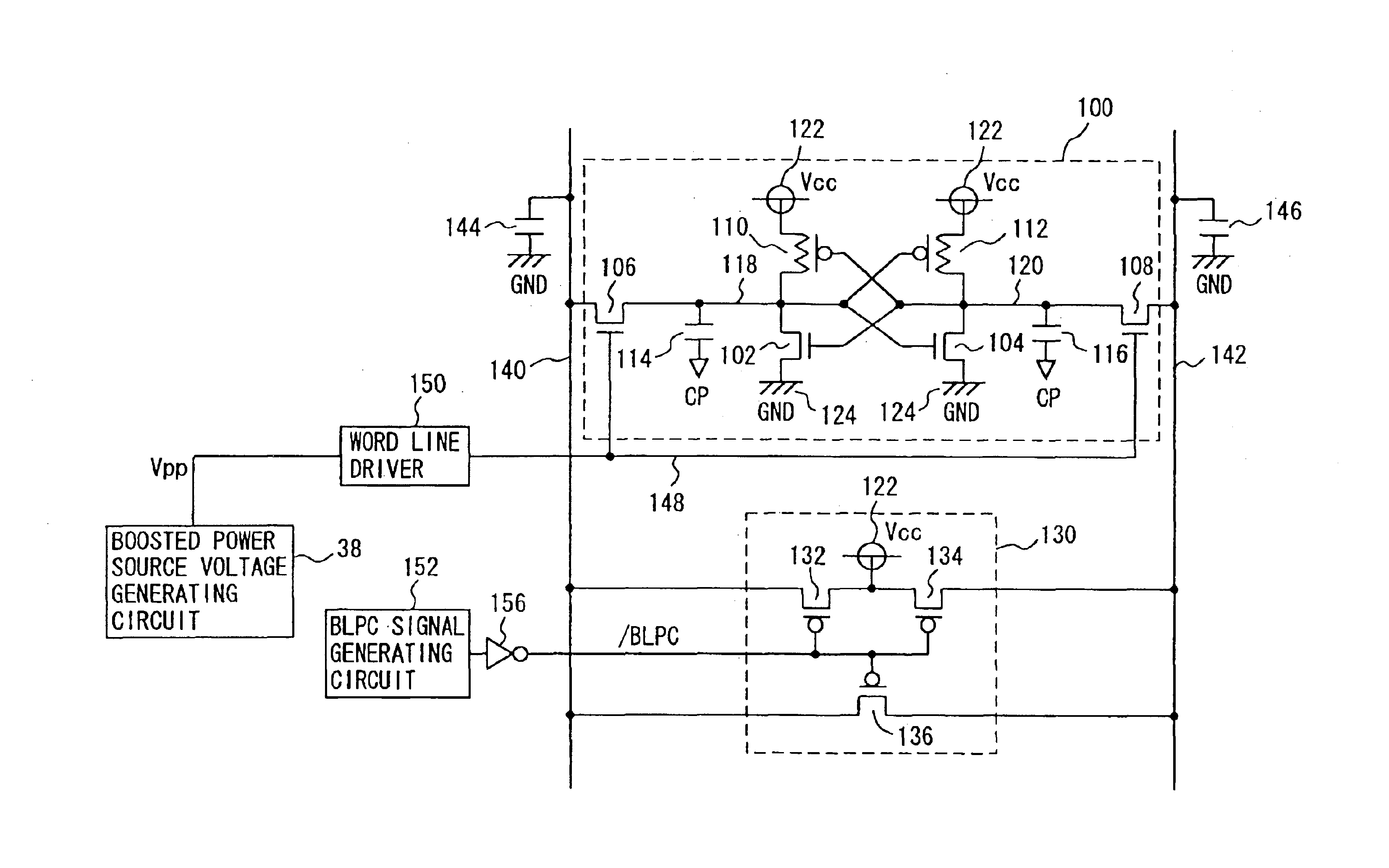
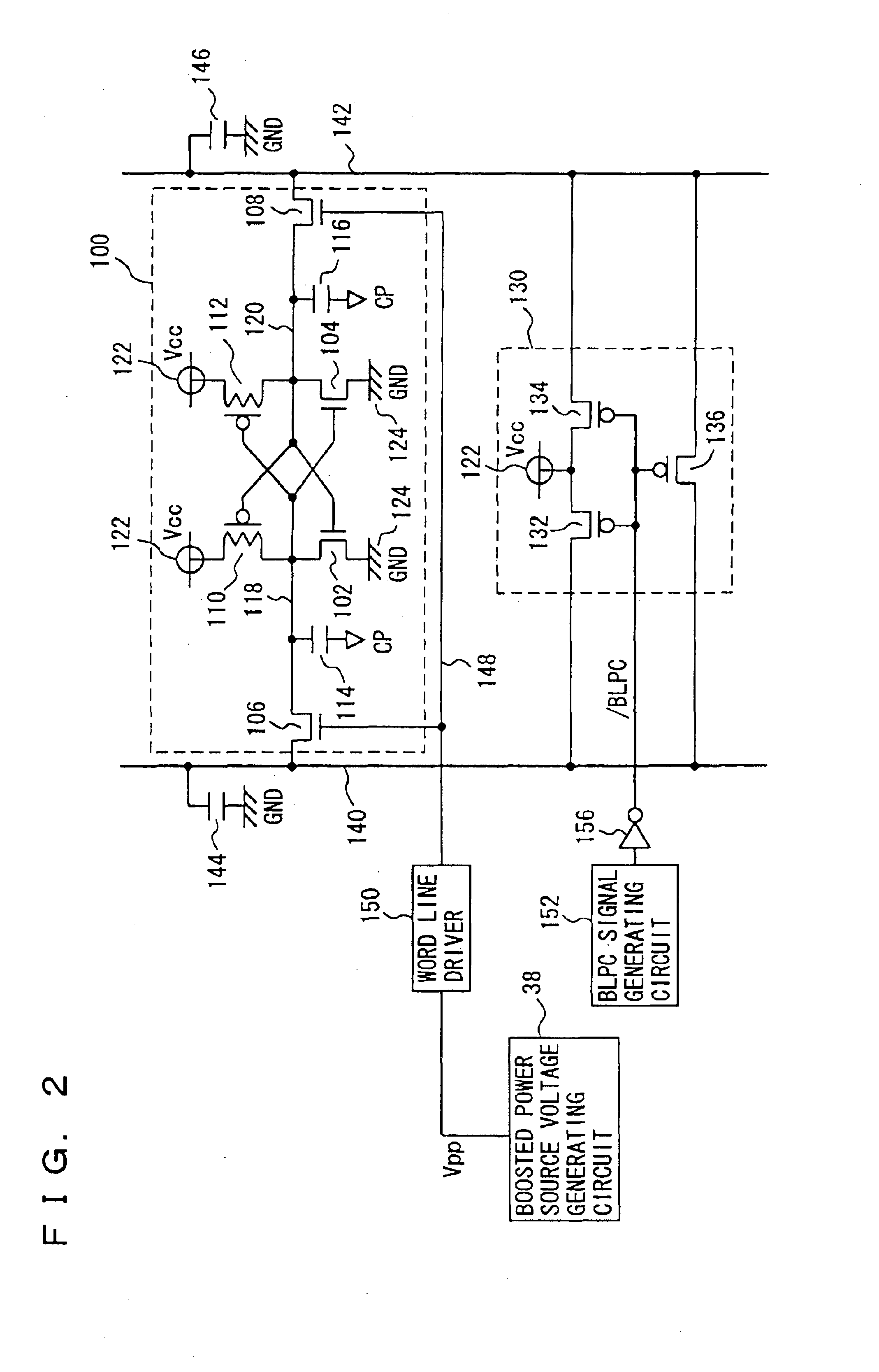
FIG. 7 is a circuit diagram showing the configuration of one of memory cells arranged in a matrix in memo...

third embodiment

FIG. 8 is a general block diagram conceptually showing the configuration of a semiconductor memory device 10B according to a third embodiment of the present invention.

Referring to FIG. 8, semiconductor memory device 10B has a configuration similar to that of semiconductor memory device 10 according to the first embodiment shown in FIG. 1 except that a step-down power source generating circuit 40 is further provided and a boosted power source voltage generating circuit 38B and a memory cell array 36A are provided in place of boosted power source voltage generating circuit 38 and memory cell array 36, respectively.

Step-down power source generating circuit 40 receives power source voltage Vcc and ground voltage Vss from power source terminal 20, generates a voltage VDC which is a predetermined potential, and outputs generated voltage VDC to boosted power source voltage generating circuit 38A, a not-shown bit line precharge circuit, and a memory cell included in memory cell array 36A. S...


PUM


Abstract

In a memory cell, the cell ratio between an N-channel MOS transistor as a driver transistor and an N-channel MOS transistor as an access transistor is 1. To the first and second storage nodes, capacitors are connected, respectively. A word line driver receives a voltage obtained by boosting a power source voltage from a boosted power source voltage generating circuit and activates a word line with the boosted voltage. A bit line precharge circuit precharges bit lines to the power source potential when the word line is inactivated in accordance with a signal outputted from a BLPC signal generating circuit.

Description

BACKGROUND OF THE INVENTION1. Field of the InventionThe present invention relates to a semiconductor memory device, and more particularly to a semiconductor memory device having static memory cells.2. Description of the Background ArtAn SRAM (Static Random Access Memory) as one of typical semiconductor memory devices is a RAM which does not need refresh operation for holding stored data. A memory cell in an SRAM has a configuration that a flip flop obtained by cross coupling two inverters each made of a load element and a driver transistor is connected to a pair bit lines via access transistors.In a memory cell in an SRAM, potential states of two storage nodes in a flip flop correspond to stored data. For example, when potentials of two storage nodes correspond to an H logical high) level and an L (logical low) level, the state corresponds to storage data of “1” and the other state corresponds to storage data of “0”. Data on the cross-coupled storage nodes is in a bi-stable state wh...

Claims


Application Information

Patent Timeline
Patent Type & Authority Patents(United States)
IPC IPC(8): G11C11/40H01L21/70G11C11/00G11C11/41H01L27/11H01L21/8244G11C7/12G11C8/08G11C11/412G11C11/417
CPCG11C7/12G11C11/417G11C11/412G11C8/08G11C11/41
Inventor IZUTSU, TAKASHI
Owner RENESAS ELECTRONICS CORP
Why Eureka
Try Eureka