Semiconductor device

a technology of semiconductors and semiconductors, applied in the field of semiconductor devices, can solve the problems of consuming a lot of resources, and achieve the effects of reducing the area of a memory cell, reducing the manufacturing cost per unit storage capacity, and reducing the area per bi

Active Publication Date: 2016-03-03
SEMICON ENERGY LAB CO LTD
View PDF7 Cites 5 Cited by
  • Summary
  • Abstract
  • Description
  • Claims
  • Application Information

AI Technical Summary

Benefits of technology

[0006]In the case of a storage device, its miniaturization reduces the area of a memory cell, so that the manufacturing cost per unit storage capacity can be reduced. In the case of a flash memory, more than 1 bit of data, that is, multilevel data is stored in a memory cell, whereby the area per bit is reduced and thus the manufacturing cost per unit storage capacity can be reduced.

Problems solved by technology

In this method, however, written pieces of data are sequentially read out to verify whether each piece of data corresponds to a desired data, so that it takes a long time for data writing.
Particularly in the case where multilevel data is stored in a memory cell, the threshold voltage needs to fall within a narrow range; thus, it takes an extremely long time for data writing.

Method used


Image

  • Semiconductor device
  • Semiconductor device
  • Semiconductor device

Examples


embodiment 1

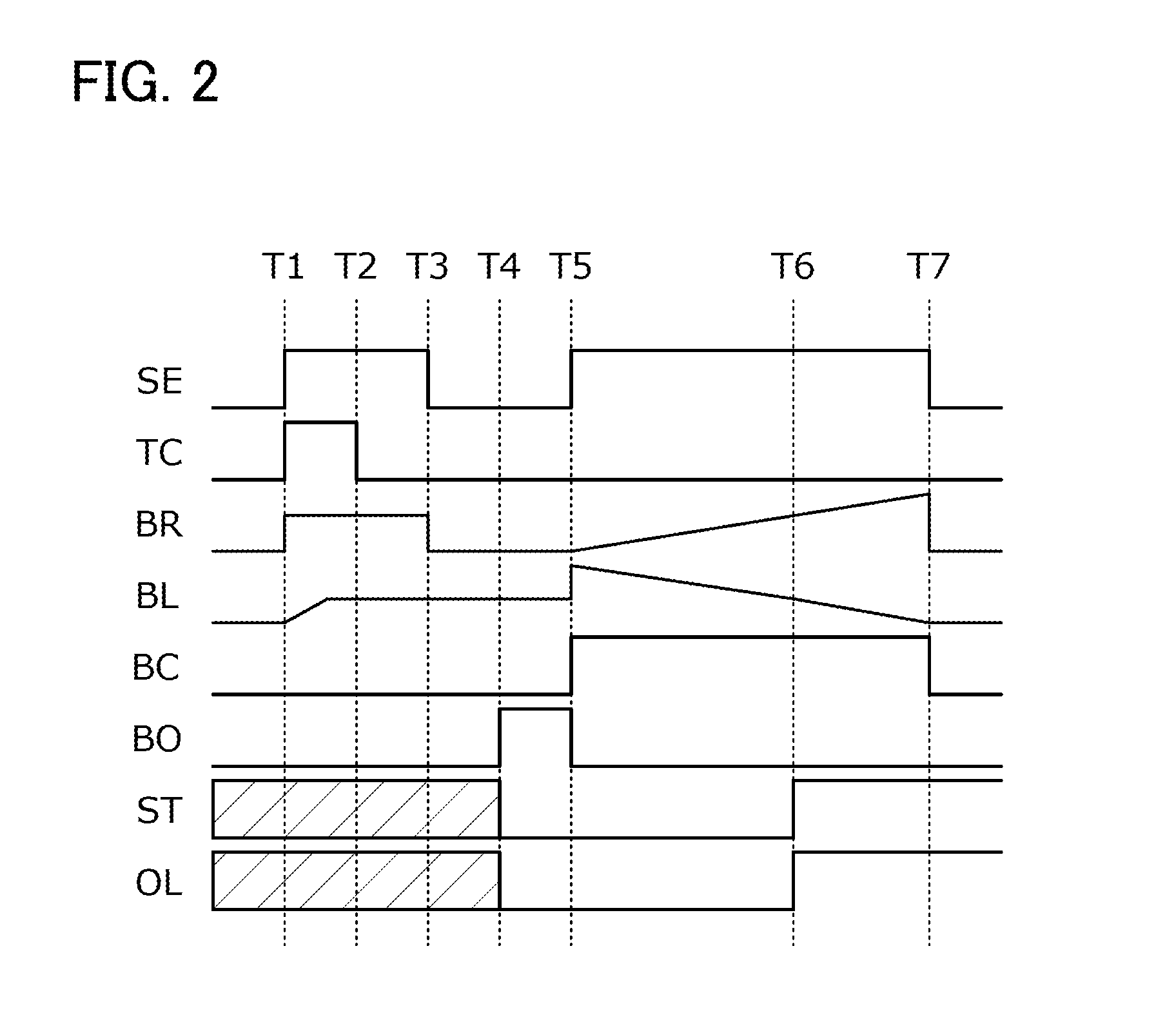
[0058]A semiconductor device of one embodiment of the present invention will be described with reference to FIGS. 1A and 1B, FIG. 2, and FIG. 3.

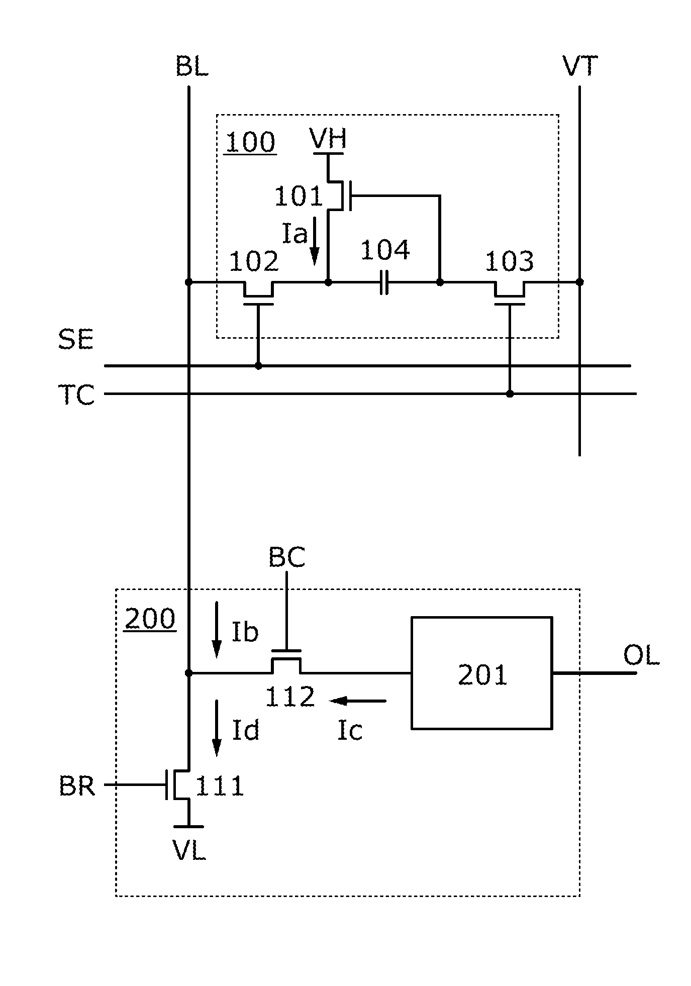
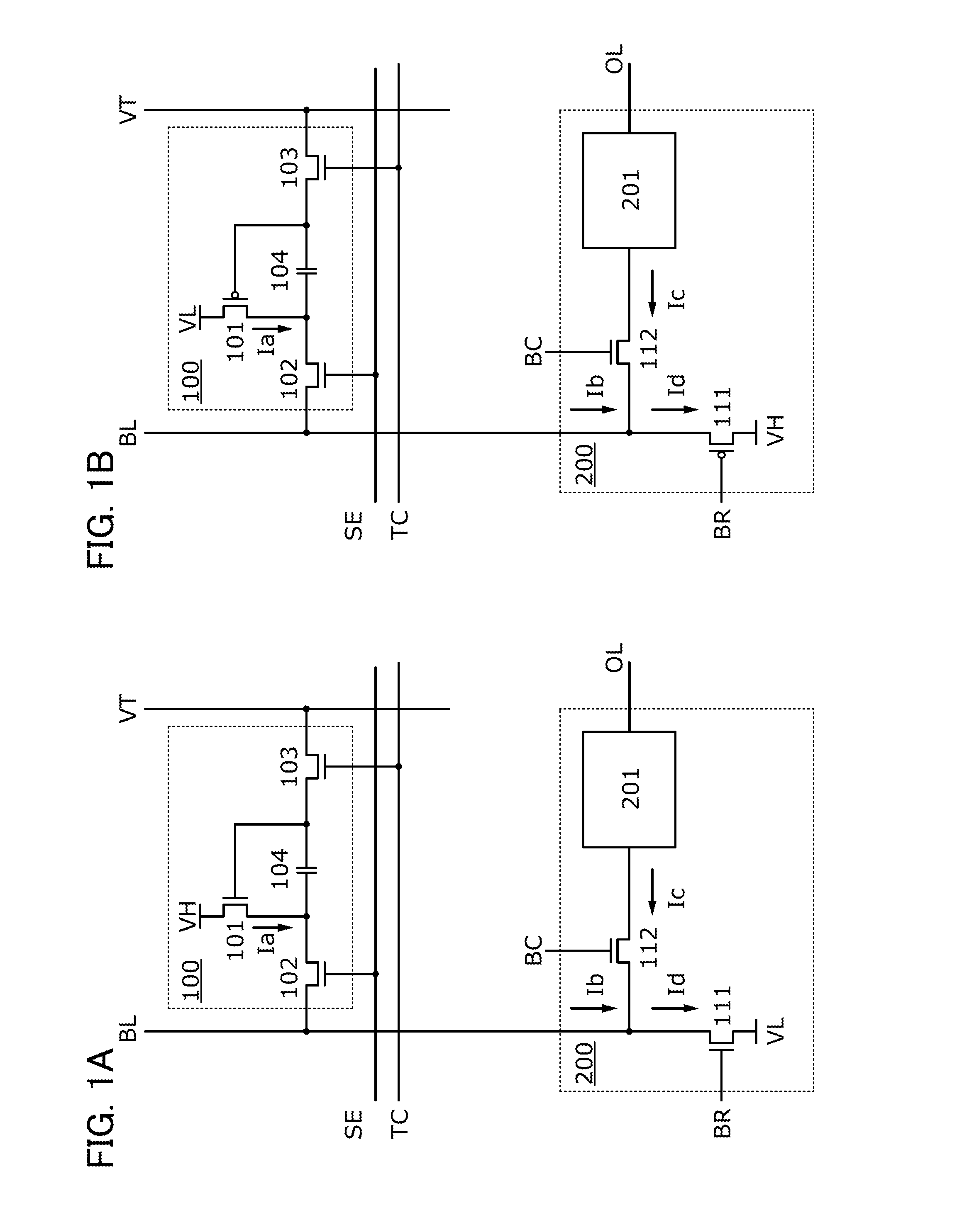
[0059]FIG. 1A illustrates a configuration example of a memory cell 100 and a write / read circuit 200.

[0060]The memory cell 100 includes a transistor 101, a transistor 102, a transistor 103, and a capacitor 104. To the memory cell 100, a voltage is supplied through a wiring VH and a wiring VT, and control signals are supplied through a wiring SE and a wiring TC. Data of the memory cell is input to and output from a wiring BL.

[0061]A drain of the transistor 101 is connected to the wiring VH. A source of the transistor 101 is connected to a first terminal of the capacitor 104 and a source of the transistor 102. A gate of the transistor 101 is connected to a second terminal of the capacitor 104 and a drain of the transistor 103. A drain of the transistor 102 is connected to the wiring BL. A gate of the transistor 102 is connected to the wiring SE...

embodiment 2

[0095]In this embodiment, an example of a semiconductor device including the memory cell described in Embodiment 1 will be described.

[0096]FIG. 4 is a block diagram illustrating a configuration example of a semiconductor device.

[0097]A semiconductor device 300 illustrated in FIG. 4 includes a memory cell array 301, a row driver 302, and a column driver 303.

[0098]The memory cell array 301 is provided with a plurality of memory cells 100, a plurality of wirings SE, a plurality of wirings TC, a plurality of wirings BL, and a plurality of wirings VT. The memory cells 100 are arranged in a matrix of m rows and n columns (m and n are integers of 2 or more). There are typically illustrated in FIG. 4 four memory cells 100, a wiring SE[m−1] as a word select line for an (m−1)-th row, a wiring TC[m−1] as a word control line for an (m−1)-th row, a wiring SE[m] as a word select line for an m-th row, a wiring TC[m] as a word control line for an m-th row, a wiring BL[n−1] as a bit line for an (n−1...

embodiment 3

[0132]In this embodiment, examples of OS transistors which can be used in the semiconductor device described in Embodiment 1 will be described.

[0133]FIGS. 9A to 9D are a top view and cross-sectional views of a transistor 600. FIG. 9A is the top view. FIG. 9B illustrates a cross section along the dashed-dotted line Y1-Y2 in FIG. 9A. FIG. 9C illustrates a cross section along the dashed-dotted line X1-X2 in FIG. 9A. FIG. 9D illustrates a cross section along the dashed-dotted line X3-X4 in FIG. 9A. In FIGS. 9A to 9D, some components are scaled up or down or omitted for easy understanding. In some cases, the direction of the dashed-dotted line Y1-Y2 is referred to as a channel length direction and the direction of the dashed-dotted line X1-X2 is referred to as a channel width direction.

[0134]Note that the channel length refers to, for example, a distance between a source (source region or source electrode) and a drain (drain region or drain electrode) in a region where a semiconductor (o...


PUM


Abstract

To provide a memory cell for storing multilevel data that is less likely to be affected by variations in characteristics of transistors and that is capable of easily writing multilevel data in a short time and accurately reading it out. In writing, a current corresponding to multilevel data is supplied to the transistor in the memory cell and stored as the gate-drain voltage of the transistor in the memory cell. In reading, a current is supplied to the transistor in the transistor with the stored gate-drain voltage, and the multilevel data is obtained from the voltage supplied to generate a current that is equal to the current.

Description

BACKGROUND OF THE INVENTION[0001]1. Field of the Invention[0002]One embodiment of the present invention relates to a semiconductor device, a method for operating the semiconductor device, or the like. For example, one embodiment of the present invention relates to a storage device, a method for operating the storage device, or the like.[0003]Note that one embodiment of the present invention is not limited to the above technical field. The technical field of one embodiment of the invention disclosed in this specification and the like relates to an object, a method, or a manufacturing method. One embodiment of the present invention relates to a process, a machine, manufacture, or a composition of matter. Specifically, examples of the technical field of one embodiment of the present invention disclosed in this specification include a semiconductor device, a display device, a liquid crystal display device, a light-emitting device, a lighting device, a power storage device, a storage dev...

Claims


Application Information

Patent Timeline
Patent Type & Authority Applications(United States)
IPC IPC(8): H01L27/115H01L23/528H01L27/06H01L29/786
CPCH01L27/11526H01L29/7869H01L23/528H01L27/0629G11C11/565G11C2029/0403H01L21/8258H01L27/0688H01L27/1207H01L27/146H10B41/70G11C11/34G11C11/402G11B13/00
Inventor KUROKAWA, YOSHIYUKI
Owner SEMICON ENERGY LAB CO LTD
Why Eureka
Try Eureka