Multi-valued ROM using carbon-nanotube and nanowire fet

a technology of carbon nanotubes and nanowires, applied in the field of memory devices, can solve the problems of reduced storage area and compact design, and achieve the effects of reduced storage area, compact design, and reduced power consumption

Inactive Publication Date: 2011-03-17
TOSHIBA AMERICA RES
View PDF9 Cites 2 Cited by
  • Summary
  • Abstract
  • Description
  • Claims
  • Application Information

AI Technical Summary

Benefits of technology

According to an embodiment of the invention, multi-valued ROM cells are created by controlling the number of nanotube / nanowire channels in carbon nanotube and nanowire FETs (CNFET / NWFET), in order to store different values in the memory cell. This leads to a reduced area of the memory cell, resulting in a smaller and more compact design. Further, this smaller design allows for a low power consumption and high performance of the memory cell.

Problems solved by technology

This leads to a reduced area of the memory cell, resulting in a smaller and more compact design.

Method used


Image

  • Multi-valued ROM using carbon-nanotube and nanowire fet
  • Multi-valued ROM using carbon-nanotube and nanowire fet
  • Multi-valued ROM using carbon-nanotube and nanowire fet

Examples


first embodiment

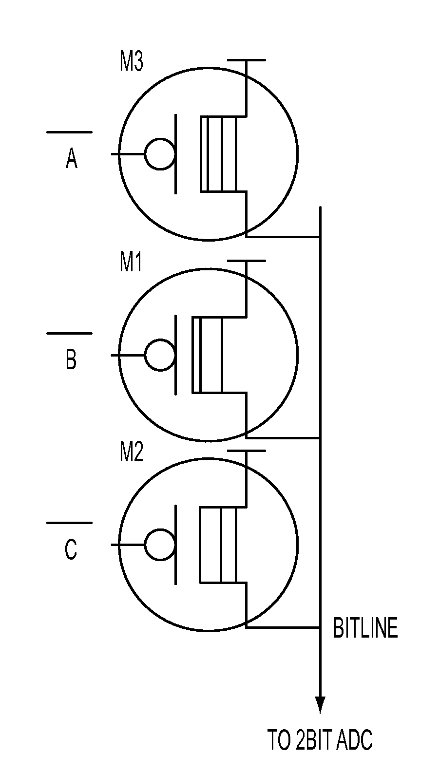
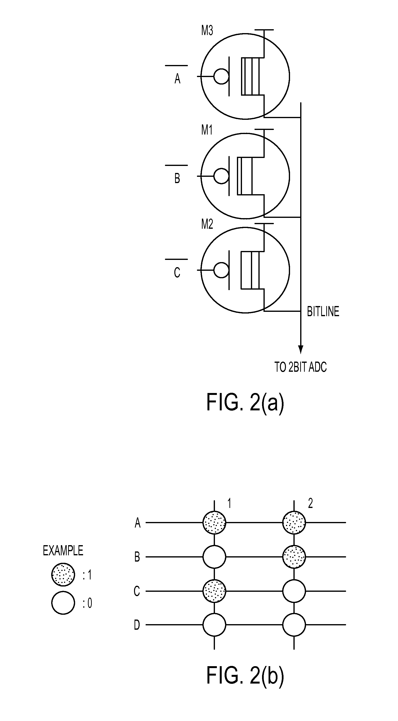
FIG. 3(a) shows a possible way of implementing CNFETs / NWFETs with a different number of CNTs in the transistor channel, according to a Although shown using CNTs, NWs can also be used, either entirely, or together with CNTs. FIG. 3(a) shows a possible layout design of three transistors, as shown in FIG. 2, with one CNT per state. In this technique, by selecting the gate, the number of CNTs, through which current flows, can be conveniently controlled.

As shown in FIG. 3(a), a ROM 20 has multivalued transistors 21, 22 and 23, positioned adjacent to each other. Gate 2A is part of transistor 21, gate 2B is part of transistor 22 and gate 2C is part of transistor 23. A voltage source VDD 18 is shown along the top edge of gate 2A and in between gates 2B and 2C. A bitline 16A is shown between gates 2A and 2B, and a bitline 16B is shown along the bottom edge of gate 2C. Both VDD 18 and bitline 16 are conductors.

CNTs 8 are positioned across VDD 18 and gates 2A, 2B and 2C. As shown in FIG. 3(a)...

second embodiment

FIG. 4 shows a multi-valued ROM 25 using a CNT / NW channel. The general layout of FIG. 4 is similar to that shown in FIG. 3(a), however, the embodiment uses sets of three CNTs, 9A, 9B and 9C to distinguish amongst the different saved data. That is, instead of using a single CNT to represent a piece of saved data or a different data state, this embodiment uses 3 CNTs to represent a piece of saved data or a different data state.

However, the embodiment is not limited to three CNTs. Two CNTs, four CNTs or more could be used to represent a saved piece of data, depending on the desired resolution. The more CNTs are used to represent a single piece of data, the larger the difference in current will be from one state to another state, thus providing a higher resolution. However, the more CNTs are used to represent a single piece of data, the more power is used.

third embodiment

FIG. 5 shows a third embodiment using a memory block 27 with a single CNT or nanowire. In this embodiment, different states are implemented using multiple fingers as a gate. The operation of the device is similar to that discussed above regarding the embodiment shown in FIG. 3(a).

When reading the memory of transistor 41, a voltage is applied to gate 2A. A current will then flow from VDD 18A, through CNT 8 and into bitlines 16A and 16B. Further, a current will flow from VDD 18B, through CNT 8 and into bitline 16B. Thus, three units of current will flow into bitline 16.

When reading the memory of transistor 42, a voltage is applied to gate 2C. A current will then flow from VDD 18B, through CNT 8 and into bitline 16C. A current will also flow from VDD 18C, through CNT 8 and into bitline 16C. Thus, two units of current will flow into bitline 16.

When reading the memory of transistor 43, a voltage is applied to gate 2B. A current will then flow from VDD 18C, through CNT 8 and into bitline ...


PUM

PropertyMeasurementUnit
currentaaaaaaaaaa
currentaaaaaaaaaa
currentaaaaaaaaaa

Abstract

A multivalued memory device which includes a first multivalued memory transistor and a second multivalued memory transistor, wherein each transistor has a channel made from at least one carbon nanotube or nanowire, wherein data is stored by varying the number of carbon nanotubes or nanowires used in the channel, wherein the channel is the at least one carbon nanotube or nanowire which allows current to flow through it.

Description

BACKGROUND1. Field of the InventionThe present invention relates, e.g., to memory devices and, in preferred embodiments, to a multi-valued memory device using carbon nanotube and nanowire FET.2. Background DiscussionThe following description sets forth the inventor's knowledge of related art and problems therein and should not be construed as an admission of knowledge in the prior art. Throughout this disclosure, the phrases carbon nanotube (CNT) and nanowire (NW) will be used interchangeably. For the purposes of this disclosure, both CNTs and NWs can be used interchangeably.Traditionally a memory cell stores only 1 bit (binary) of information, i.e., either ‘0’ or ‘1’. However, if the memory cell is capable of storing more values besides ‘0’ or ‘1’ (known as a multi-valued memory cell), the overall memory size can be significantly reduced compared to a memory consisting of 1 bit cells for storing a similar amount of information. That is, traditionally the storage capacity of a memor...

Claims


Application Information

Patent Timeline
Patent Type & Authority Applications(United States)
IPC IPC(8): G11C16/04
CPCB82Y10/00G11C11/5692G11C13/025G11C17/16G11C17/165H01L51/0512H01L27/112H01L29/0665H01L29/0673H01L29/685H01L51/0048G11C2213/17H10B20/00H10K85/221H10K10/462
Inventor PAUL, BIPUL C.
Owner TOSHIBA AMERICA RES
Why Eureka
Try Eureka